
CEITEC Nano Research Infrastructure
Brno University of Technology
Purkyňova 123, 612 00 Brno
Czech Republic
 +420 54114 9207
 nano@ceitec.vutbr.cz
Consumables | ShP | today | feedback


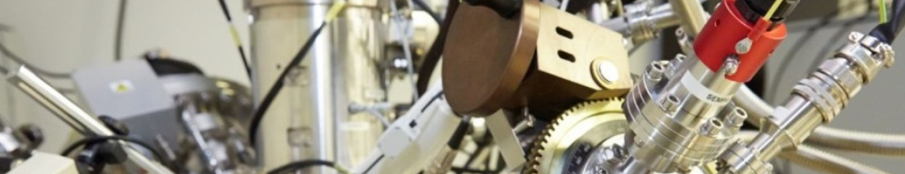
Scanning Electron Microscope/E-beam writer TESCAN MIRA3Raith LIS (MIRA-EBL)

Guarantor:
Vojtěch Švarc, Ph.D.
Instrument status:
![]() Operational, 16.7.2025 17:18
Operational, 16.7.2025 17:18
Equipment placement:
CEITEC Nano - C1.29
SEM is a type of microscope where a focused beam of electrons is scanned over the sample to generate an image or to modify the sample surface in nanometric resolution (usually better than 10 nm). The sample image is generated by detecting secondary and backscattered electrons emitted from the impact location of the beam. The tool is preferred for e-beam lithography, where the resist-coated sample is selectively exposed to the electron beam, allowing the preparation of very small patterns (< 50 nm and less) in the resistant surface. There can be further processing of the sample by wet chemistry (development, stripping). An interferometric stage can also be used to achieve ultimate resolution of electron beam lithography over a large area and to join more fields together.
Publications:
-
TAKHSHA GHAHFAROKHI, M.; HORKÝ, M.; NASI, L.; KOSOGOR, A.; TREVISI, G.; CASOLI, F.; ARREGI URIBEETXEBARRIA, J.; BRESCIA, R.; UHLÍŘ, V.; ALBERTINI, F., 2025: Spatially confined magnetic shape-memory Heuslers: Implications for nanoscale devices. ACTA MATERIALIA 284, p. 1 - 11, doi: 10.1016/j.actamat.2024.120579; FULL TEXT
(VERIOS, MIRA-EBL, RIE-FLUORINE, VERSALAB, WIRE-BONDER) -
DODD, S.; GUDINO, N.; ZADOROZHNII, O.; STAŇO, M.; HAJDUČEK, J.; ARREGI URIBEETXEBARRIA, J.; MORRIS, H.; UHLÍŘ, V.; BARBIC, M.; KORETSKY, A., 2025: Field switching of microfabricated metamagnetic FeRh MRI contrast agents. SCIENTIFIC REPORTS 15(1), p. 1 - 10, doi: 10.1038/s41598-025-85384-6; FULL TEXT
(MAGNETRON, VERSALAB, MIRA-EBL, EVAPORATOR, RIE-FLUORINE, ICON-SPM, KERR-MICROSCOPE) -
Wang, Y.; Guo, M.; Davídková, K.; Verba, R.; Guo, X.; Dubs, C.; Chumak, A. V.; Pirro, P.; Wang, Q., 2025: Fast switchable unidirectional forward volume spin-wave emitter. PHYSICAL REVIEW APPLIED 23(1), p. 1 - 10, doi: 10.1103/PhysRevApplied.23.014066; FULL TEXT
(MIRA-EBL, RIE-FLUORINE, SCIA, EVAPORATOR) -
Davídková, K.; Levchenko, K.; Bruckner, F. ; Verba, R.; Majcen, F.; Wang, Q.; Lindner, M.; Dubs, C.; Vlaminck, V.; Klíma, J.; Urbánek, M.; Suess, D.; Chumak, A., 2025: Nanoscale spin-wave frequency-selective limiter for 5G technology. PHYSICAL REVIEW APPLIED 23(3), doi: 10.1103/PhysRevApplied.23.034026; FULL TEXT
(VNA-MPI, MIRA-EBL, EVAPORATOR) -
ZENBAA, N.; LEVCHENKO, K.; PANDA, J.; DAVÍDKOVÁ, K.; RUHWEDEL, M.; KNAUER, S.; LINDNER, M.; DUBS, C.; WANG, Q.; URBÁNEK, M.; PIRRO, P.; CHUMAK, A., 2025: YIG/CoFeB Bilayer Magnonic Isolator. IEEE MAGNETICS LETTERS 16, p. 1 - 5, doi: 10.1109/LMAG.2025.3551990; FULL TEXT
(VNA-MPI, BRILLOUIN, MIRA-EBL, EVAPORATOR, RAITH)
-
Horký, M., 2025: Controlling the magnetic phase transition in spatially confined structures. PH.D. THESIS , p. 1 - 181; FULL TEXT
(RAITH, MIRA-EBL, LYRA, TEGRAMIN, SUSS-MA8, DEKTAK, NANOCALC, MAGNETRON, EVAPORATOR, RIE-FLUORINE, WIRE-BONDER, MPS150, CRYOGENIC, LAKESHORE, VERSALAB, ICON-SPM, UHV-PREPARATION, TITAN, HELIOS, VERIOS, RIGAKU3, RIGAKU9) -
SUPALOVÁ, L.; BARTOŠÍK, M.; ŠVARC, V.; MACH, J.; PIASTEK, J.; ŠPAČEK, O.; KONEČNÝ, M.; ŠIKOLA, T., 2025: High-Temperature Ultrasensitive FET-Based CVD Graphene Hall Probes. ACS APPLIED ELECTRONIC MATERIALS 7(13), p. 5889 - 5897, doi: 10.1021/acsaelm.5c00351; FULL TEXT
(DWL, SUSS-MA8, EVAPORATOR, MIRA-EBL, RIE-FLUORINE, WIRE-BONDER, WITEC-RAMAN, LYRA) -
DAVÍDKOVÁ, K.; LEVCHENKO, K.; SERHA, R.; BRUCKNER, F.; LINDNER, M.; DUBS, C.; URBÁNEK, M.; SUESS, D.; WANG, Q.; VERBA, R.; CHUMAK, A., 2025: Spin-wave microscale RF delay lines for mid- and high-frequency 5G band. JOURNAL OF APPLIED PHYSICS 138(14), p. 1 - 14, doi: 10.1063/5.0286108; FULL TEXT
(VNA-MPI, MIRA-EBL, EVAPORATOR) -
JANČÍK PROCHÁZKOVÁ, A.; MICHÁLKOVÁ, H.; ČÍHALOVÁ, K.; HEGER, Z.; PUMERA, M., 2025: Microrobots for Antibiotic-Resistant Staphylococcus aureus Skin Colony Eradication. ACS APPLIED MATERIALS & INTERFACES 17(27), p. 39340 - 39348, doi: 10.1021/acsami.5c08683; FULL TEXT
(LEICACOAT-STAN, RIGAKU3, MIRA-EBL) -
Děcký, M., 2025: Combined detector for visible and infrared radiation. MASTER´S THESIS , p. 1 - 63; FULL TEXT
(MIRA-EBL, SUSS-MA8, DEKTAK, NANOCALC, MAGNETRON, RIE-FLUORINE, EVAPORATOR, WIRE-BONDER, MPS150, LYRA, LASER-DICER) -
KOVAŘÍK, M.; CITTERBERG, D.; PAIVA DE ARAÚJO, E.; ŠIKOLA, T.; KOLÍBAL, M., 2024: Understanding the Effect of Electron Irradiation on WS2 Nanotube Devices to Improve Prototyping Routines. ACS APPLIED ELECTRONIC MATERIALS 6(12), p. 8776 - 7, doi: 10.1021/acsaelm.4c01450; FULL TEXT
(ALD-FIJI, MIRA-EBL, EVAPORATOR, MPS150, KEITHLEY-4200, LYRA, LITESCOPE-LYRA, WITEC-RAMAN, WIRE-BONDER, NANOSCAN) -
Novotný, A., 2024: Preparation of graphene membranes. BACHELOR´S THESIS , p. 1 - 53; FULL TEXT
(TITAN, MIRA-EBL, LYRA, RIE-FLUORINE, WITEC-RAMAN) -
GALLINA, P.; KVAPIL, M.; LIŠKA, J.; KONEČNÁ, A.; KŘÁPEK, V.; KALOUSEK, R.; ZLÁMAL, J.; ŠIKOLA, T., 2023: Strong coupling in an Au plasmonic antenna-SiO2 layer system: A hybrid-mode analysis. PHYSICAL REVIEW B 107(12), p. 125144 - 6, doi: 10.1103/PhysRevB.107.125144; FULL TEXT
(ALD-FIJI, EVAPORATOR, MIRA-EBL, FTIR, NANOCALC, DEKTAK, WOOLLAM-MIR, ICON-SPM) -
GALLINA, P.; KONEČNÁ, A.; LIŠKA, J.; IDROBO, J.; ŠIKOLA, T., 2023: Strongly Coupled Plasmon and Phonon Polaritons as Seen by Photon and Electron Probes. PHYSICAL REVIEW APPLIED 19(2), p. 24042 - 11, doi: 10.1103/PhysRevApplied.19.024042; FULL TEXT
(MIRA-EBL, EVAPORATOR, FTIR) -
WOJEWODA, O.; LIGMAJER, F.; HRTOŇ, M.; KLÍMA, J.; DHANKHAR, M.; DAVÍDKOVÁ, K.; STAŇO, M.; HOLOBRÁDEK, J.; KRČMA, J.; ZLÁMAL, J.; ŠIKOLA, T.; URBÁNEK, M., 2023: Observing high-k magnons with Mie-resonance-enhanced Brillouin light scattering. COMMUNICATIONS PHYSICS 6(1), p. 1 - 10, doi: 10.1038/s42005-023-01214-z; FULL TEXT
(RAITH, MIRA-EBL, EVAPORATOR, MAGNETRON, ALD-FIJI, LYRA, ICON-SPM, BRILLOUIN) -
NOVCIC, K.; IFFELSBERGER, C.; PALACIOS CORELLA, M.; PUMERA, M., 2023: Solvents dramatically influence the atomic composition and catalytic properties of Ti3C2Tx MXenes. JOURNAL OF MATERIALS CHEMISTRY A 11(25), p. 13419 - 13, doi: 10.1039/d3ta01441j; FULL TEXT
(MIRA-EBL, KRATOS-XPS) -
Kunc, J.; Morzhuk, B.; Shestopalov, M.; Fridrišek, T.; Dědič, V., 2023: Spectral current density and responsivity scaling for Fourier transform photocurrent spectroscopy. REVIEW OF SCIENTIFIC INSTRUMENTS 94(5), doi: 10.1063/5.0139027; FULL TEXT
(RAITH, MIRA-EBL, EVAPORATOR, RIE-FLUORINE) -
Klíma, J., 2023: Spin waves in non-trivial magnetic landscapes. BACHELOR´S THESIS , p. 1 - 69; FULL TEXT
(MIRA-EBL, LYRA, ICON-SPM, KERR-MICROSCOPE, BRILLOUIN, EVAPORATOR) -
BRODSKÝ, J.; GABLECH, I.; MIGLIACCIO, L.; HAVLÍČEK, M.; DONAHUE, M.; GLOWACKI, E., 2023: Downsizing the Channel Length of Vertical Organic Electrochemical Transistors. ACS APPL MATER INTER 15(22), p. 27002 - 8, doi: 10.1021/acsami.3c02049; FULL TEXT
(SUSS-MA8, EVAPORATOR, SCIA, PARYLENE-SCS, RIE-FLUORINE, MIRA-EBL, DEKTAK, ICON-SPM) -
ŠVARC, V.; BARTOŠÍK, M.; KONEČNÝ, M.; PIASTEK, J.; NEZVAL, D.; MACH, J.; ŠIKOLA, T., 2023: Side charge propagation in simultaneous KPFM and transport measurement of humidity exposed graphene FET sensor. CARBON 215, p. 118471 - 12, doi: 10.1016/j.carbon.2023.118471; FULL TEXT
(RIE-FLUORINE, EVAPORATOR, MIRA-EBL, WIRE-BONDER) -
ROVENSKÁ, K.; LIGMAJER, F.; IDESOVÁ, B.; KEPIČ, P.; LIŠKA, J.; CHOCHOL, J.; ŠIKOLA, T., 2023: Structural color filters with compensated angle-dependent shifts. OPTICS EXPRESS 31(26), p. 43048 - 9, doi: 10.1364/OE.506069; FULL TEXT
(EVAPORATOR, MIRA-EBL, RIE-CHLORINE, ALD-FIJI, SNOM-NANONICS, TUBE-FURNACE) -
LAMB-CAMARENA, S.; PORRATI, F.; KUPRAVA, A.; WANG, Q.; URBÁNEK, M.; BARTH, S.; MAKAROV, D.; HUTH, M.; DOBROVOLSKIY, O., 2023: 3D Magnonic Conduits by Direct Write Nanofabrication. NANOMATERIALS 13(13), doi: 10.3390/nano13131926; FULL TEXT
(MIRA-EBL, EVAPORATOR, BRILLOUIN) -
MILOSAVLJEVIĆ, V.; KOŠARIŠŤANOVÁ, L.; DOLEŽELÍKOVÁ, K.; ADAM, V.; PUMERA, M., 2022: Microrobots with Antimicrobial Peptide Nanoarchitectonics for the Eradication of Antibiotic-Resistant Biofilms. ADVANCED MATERIALS FOR OPTICS AND ELECTRONICS 32(43), p. 1 - 11, doi: 10.1002/adfm.202112935; FULL TEXT
(LEICACOAT-NANO, MIRA-EBL, MIRA-STAN, KRATOS-XPS) -
Fridrišek, T., 2022: Optical gating of epitaxial graphene. MASTER´S THESIS
(MIRA-EBL, RIE-FLUORINE, EVAPORATOR, WIRE-BONDER, LYRA) -
Vodička, M., 2022: Fabrication and characterisation of plasmonic antennas on selected thin film with aim to get enhanced absorption due to presence of strong coupling. BACHELOR´S THESIS , p. 1 - 60; FULL TEXT
(MIRA-EBL, FTIR, EVAPORATOR, MPS150) -
Děcký, M., 2022: Fabrication and testing of microbolometer or other infrared detector based on plasmonic antennas. BACHELOR´S THESIS , p. 1 - 44; FULL TEXT
(LYRA, MIRA-EBL, EVAPORATOR, DWL, MPS150) -
Turčan, I., 2022: Magnetism in curved geometries. PH.D. THESIS , p. 1 - 117; FULL TEXT
(LYRA, BRILLOUIN, ICON-SPM, MIRA-EBL, KERR-MICROSCOPE, HELIOS) -
Vaňatka, M., 2021: Static and dynamic properties of nanostructured magnetic materials. PH.D. THESIS , p. 1 - 113; FULL TEXT
(VERSALAB, VNA-MPI, TITAN, BRILLOUIN, MIRA-EBL, RAITH, KERR-MICROSCOPE, MAGNETRON, EVAPORATOR, VERIOS, WIRE-BONDER, LYRA) -
USSIA, M.; URSO, M.; DOLEŽELÍKOVÁ, K.; MICHÁLKOVÁ, H.; ADAM, V.; PUMERA, M., 2021: Active Light-powered antibiofilm ZnO micromotors with chemically programmable properties. ADVANCED FUNCTIONAL MATERIALS 31(27), p. 1 - 10, doi: 10.1002/adfm.202101178; FULL TEXT
(MIRA-EBL, RIGAKU9, KRATOS-XPS) -
Hajduček, J., 2021: Imaging of metamagnetic thin films using TEM. MASTER´S THESIS , p. 1 - 78; FULL TEXT
(MAGNETRON, VERSALAB, MIRA-EBL, HELIOS, TITAN) -
KEPIČ, P.; LIGMAJER, F.; HRTOŇ, M.; REN, H.; MENEZES, L.; MAIER, S.; ŠIKOLA, T., 2021: Optically Tunable Mie Resonance VO2 Nanoantennas for Metasurfaces in the Visible. ACS PHOTONICS 8(4), p. 1048 - 10, doi: 10.1021/acsphotonics.1c00222; FULL TEXT
(EVAPORATOR, MIRA-EBL, WITEC-RAMAN, WOOLLAM-VIS) -
Dhankhar, M.;, 2021: Magnetic vortex based memory device. PH.D. THESIS , p. 1 - 100; FULL TEXT
(KERR-MICROSCOPE, DWL, MIRA-EBL, RAITH, KAUFMAN, EVAPORATOR, MAGNETRON, ALD-FIJI, WIRE-BONDER, SUSS-RCD8, ICON-SPM) -
Kepič, P., 2021: Design and fabrication of tunable dielectric metasurfaces for visible and infrared wavelengths. MASTER´S THESIS , p. 1 - 76; FULL TEXT
(MIRA-EBL, EVAPORATOR, DEKTAK, WITEC-RAMAN, SNOM-NANONICS, LYRA, ICON-SPM, KRATOS-XPS) -
Pejchal, T., 2021: Towards highly-doped Ge and ZnO nanowires: Growth, characterization and doping level analysis. PH.D. THESIS ; FULL TEXT
(NANOSAM, WITEC-RAMAN, UHV-DEPOSITION, UHV-PREPARATION, VERIOS, HELIOS, TITAN, ALD-FIJI, EVAPORATOR, MIRA-EBL, MPS150, KRATOS-XPS) -
Idesová, B., 2021: Plasmonically active nanostructures for optical filtering. BACHELOR´S THESIS , p. 1 - 47; FULL TEXT
(EVAPORATOR, MIRA-EBL, FTIR) -
KŘÁPEK, V.; KONEČNÁ, A.; HORÁK, M.; LIGMAJER, F.; STÖGER-POLLACH, M.; HRTOŇ, M.; BABOCKÝ, J.; ŠIKOLA, T., 2020: Independent engineering of individual plasmon modes in plasmonic dimers with conductive and capacitive coupling. NANOPHOTONICS 9(3), p. 623 - 10, doi: 10.1515/nanoph-2019-0326; FULL TEXT
(HELIOS, MIRA-EBL, TITAN, LEICACOAT-STAN, FTIR, EVAPORATOR) -
Horák, M., 2020: Electron microscopy and spectroscopy in plasmonics. PH.D. THESIS , p. 1 - 129; FULL TEXT
(TITAN, HELIOS, VERIOS, LEICACOAT-STAN, EVAPORATOR, MAGNETRON, MIRA-EBL, LYRA, ICON-SPM) -
Wojewoda, O.; Hula, T.; Flajsman, L.; Vanatka, M.; Gloss, J.; Holobradek, J.; Stano, M.; Stienen, S.; Korber, L.; Schultheiss, K.; Schmid, M.; Schultheiss, H.; Urbanek, M , 2020: Propagation of spin waves through a Neel domain wall. APPLIED PHYSICS LETTERS 117(2), p. 022405-1 - 5, doi: 10.1063/5.0013692; FULL TEXT
(EVAPORATOR, KERR-MICROSCOPE, BRILLOUIN, MIRA-EBL, LYRA, ICON-SPM) -
Rovenská, K., 2020: Dielectric metasurfaces as modern optical components. MASTER´S THESIS , p. 1 - 57
(MAGNETRON, DEKTAK, MIRA-EBL, EVAPORATOR, VERIOS, RIE-FLUORINE, ALD-FIJI, KRATOS-XPS) -
LIŠKA, J.; LIGMAJER, F.; PINHO NASCIMENTO, P.; KEJÍK, L.; KVAPIL, M.; DVOŘÁK, P.; HORKÝ, M.; LEITNER, N.; REIMHULT, E.; ŠIKOLA, T., 2020: Effect of deposition angle on fabrication of plasmonic gold nanocones and nanodiscs. MICROELECTRONIC ENGINEERING 228, p. 1 - 6, doi: 10.1016/j.mee.2020.111326; FULL TEXT
(EVAPORATOR, RIE-FLUORINE, MIRA-EBL, LYRA, ICON-SPM) -
Babocký, J., 2020: Fabrication and characterization of nanostructures with functional properties in the field of plasmonics. PH.D. THESIS , p. 1 - 104; FULL TEXT
(MIRA-EBL, RAITH, EVAPORATOR, SNOM-NANONICS, ICON-SPM) -
Wojewoda, O., 2020: Phase-resolved Brillouin light scattering: development and applications. MASTER´S THESIS ; FULL TEXT
(BRILLOUIN, EVAPORATOR, MIRA-EBL, KERR-MICROSCOPE, LYRA, ICON-SPM) -
Hajduček, J., 2019: Substrate-controlled nucleation of the magnetic phase transtition in nanostructures. BACHELOR´S THESIS , p. 1 - 46
(MAGNETRON, CRYOGENIC, MIRA-EBL, RIE-FLUORINE, EVAPORATOR, VERSALAB, ICON-SPM) -
Hegrová, V., 2019: Application of correlative AFM/SEM microscopy. MASTER´S THESIS , p. 1 - 64
(LITESCOPE-LYRA, MIRA-EBL, RIE-FLUORINE, EVAPORATOR, WIRE-BONDER, LYRA) -
Citterberg, D., 2019: Integration of nanostuctures into functional devices. MASTER´S THESIS , p. 1 - 50
(MIRA-EBL, EVAPORATOR, WITEC-RAMAN, WIRE-BONDER, TITAN, MPS150) -
Jaskowiec, J., 2019: Spatial confinement effects in metamagnetic nanostructures. MASTER´S THESIS , p. 1 - 55
(MAGNETRON, MIRA-EBL, RAITH, CRYOGENIC, VERSALAB, ICON-SPM) -
BOUCHAL, P.; DVOŘÁK, P.; BABOCKÝ, J.; BOUCHAL, Z.; LIGMAJER, F.; HRTOŇ, M.; KŘÁPEK, V.; FAßBENDER, A.; LINDEN, S.; CHMELÍK, R.; ŠIKOLA, T., 2019: High-Resolution Quantitative Phase Imaging of Plasmonic Metasurfaces with Sensitivity down to a Single Nanoantenna. NANO LETTERS 19(2), p. 1242 - 9, doi: 10.1021/acs.nanolett.8b04776; FULL TEXT
(EVAPORATOR, MIRA-EBL, VERIOS) -
ARREGI URIBEETXEBARRIA, J.; HORKÝ, M.; FABIANOVÁ, K.; TOLLEY, R.; FULLERTON, E.; UHLÍŘ, V., 2018: Magnetization reversal and confinement effects across the metamagnetic phase transition in mesoscale FeRh structures. JOURNAL OF PHYSICS D - APPLIED PHYSICS 51(10), p. 1 - 12, doi: 10.1088/1361-6463/aaaa5a; FULL TEXT
(MIRA-EBL, MAGNETRON, LYRA) -
HORÁK, M.; BUKVIŠOVÁ, K.; ŠVARC, V.; JASKOWIEC, J.; KŘÁPEK, V.; ŠIKOLA, T., 2018: Comparative study of plasmonic antennas fabricated by electron beam and focused ion beam lithography. SCIENTIFIC REPORTS 8(1), p. 9640 - 8, doi: 10.1038/s41598-018-28037-1; FULL TEXT
(TITAN, HELIOS, MIRA-EBL, EVAPORATOR, ICON-SPM) -
Procházka, P., 2018: Fabrication of graphene and study of its physical properties. PH.D. THESIS , p. 1 - 139
(ALD-FIJI, DIENER, EVAPORATOR, MIRA-EBL, PECVD, WIRE-BONDER) -
DHANKHAR, M.; VAŇATKA, M.; URBÁNEK, M., 2018: Fabrication of Magnetic Nanostructures on Silicon Nitride Membranes for Magnetic Vortex Studies Using Transmission Microscopy Techniques. JOURNAL OF VISUALIZED EXPERIMENTS : JOVE (137), p. 1 - 7, doi: 10.3791/57817; FULL TEXT
(MIRA-EBL, EVAPORATOR, TITAN, KAUFMAN) -
Křižáková, V., 2018: Spin wave excitation and propagation in magnonic crystals prepared by focused ion beam direct writing. MASTER´S THESIS , p. 1 - 83
(HELIOS, MIRA-EBL, EVAPORATOR, WIRE-BONDER, KERR-MICROSCOPE, LYRA, ICON-SPM) -
Rovenská, K., 2018: Metallic nanostructures with three-dimensional topography for plasmonics. BACHELOR THESIS , p. 1 - 45
(MIRA-EBL, EVAPORATOR, FTIR) -
PROCHÁZKA, P.; MAREČEK, D.; LIŠKOVÁ, Z.; ČECHAL, J.; ŠIKOLA, T., 2017: X-ray induced electrostatic graphene doping via defect charging in gate dielectric. SCIENTIFIC REPORTS 7, p. 1 - 7, doi: 10.1038/s41598-017-00673-z; FULL TEXT
(MIRA-EBL, DIENER, ALD-FIJI, WIRE-BONDER) -
BABOCKÝ, J.; KŘÍŽOVÁ, A.; ŠTRBKOVÁ, L.; KEJÍK, L.; LIGMAJER, F.; HRTOŇ, M.; DVOŘÁK, P.; TÝČ, M.; ČOLLÁKOVÁ, J.; KŘÁPEK, V.; KALOUSEK, R.; CHMELÍK, R.; ŠIKOLA, T., 2017: Quantitative 3D phase imaging of plasmonic metasurfaces. ACS PHOTONICS 4(6), p. 1389
- 9, doi: 10.1021/acsphotonics.7b00022; FULL TEXT
(MIRA-EBL, EVAPORATOR, LYRA, Q-Phase) -
Turčan, I., 2017: Study of Magnonic Crystals in a Frequency Domain. MASTER´S THESIS , p. 1 - 55
(MIRA-EBL, EVAPORATOR, MAGNETRON, WIRE-BONDER) -
Holobrádek, J., 2017: Transport Properties of One Magnetic Nanostructures. BACHELOR´S THESIS , p. 1 - 48
(TITAN, MIRA-EBL, EVAPORATOR, WIRE-BONDER, CRYOGENIC, ICON-SPM) -
Citterberg, D., 2017: Preparation of contacts to one-dimensional nanostructurs. BACHELOR´S THESIS , p. 1 - 26
(DWL, MIRA-EBL, WIRE-BONDER, EVAPORATOR) -
Jaskowiec, J., 2017: Magnetic Force Microscopy and Transport Properties of Metamagnetic Nanostructures. BACHELOR´S THESIS , p. 1 - 47
(MAGNETRON, MIRA-EBL, RAITH, CRYOGENIC, LYRA, ICON-SPM) -
Vaňatka, M., 2017: Fabrication and characterization of nanostructures with functional properties in the field of spintronics. TREATISE TO STATE DOCTORAL EXAM , p. 1 - 31
(TITAN, MIRA-EBL, EVAPORATOR, MAGNETRON, WIRE-BONDER, LYRA) -
BABOCKÝ, J.; DVOŘÁK, P.; LIGMAJER, F.; HRTOŇ, M.; ŠIKOLA, T.; BOK, J.; FIALA, J., 2016: Patterning large area plasmonic nanostructures on nonconductive substrates using variable pressure electron beam lithography. JOURNAL OF VACUUM SCIENCE & TECHNOLOGY B 34(6), p. 06K801-1 - 4, doi: 10.1116/1.4966959; FULL TEXT
(MIRA-EBL) -
Musálek, T., 2016: Semiconductor nanowire growth utilizing alloyed catalyst. MASTER’S THESIS , p. 1 - 52
(UHV-MBE, VERIOS, MIRA-EBL, ALD-FIJI, LYRA) -
Fabianová, K., 2016: Fabrication of well defined nanoporous structures with application in membrane sensing. BACHELOR’S THESIS , p. 1 - 54
(PECVD, MIRA-EBL, RIE-FLUORINE, NANOCALC, MAGNETRON, EVAPORATOR, LYRA) -
Lišková, Z., 2015: Fabrication of Nanostructures and Nanodevices for Nanoelectronics and Spintronics. PH.D. THESIS , p. 1 - 106
(MIRA-EBL, DIENER, NANOCALC, DWL, EVAPORATOR, WIRE-BONDER, ALD-FIJI, LYRA) -
Břínek, L., 2015: Application of Plasmon Polaritons in Nanophotonics. PH.D. THESIS , p. 1 - 75
(FTIR, MIRA-EBL, LYRA) -
URBÁNEK, M.; UHLÍŘ, V.; LAMBERT, C.; KAN, J.; EIBAGI, N.; VAŇATKA, M.; FLAJŠMAN, L.; KALOUSEK, R.; IM, M.; FISCHER, P.; ŠIKOLA, T.; FULLERTON, E., 2015: Dynamics and efficiency of magnetic vortex circulation reversal. PHYSICAL REVIEW B 91(9), p. 094415-1 - 11, doi: 10.1103/PhysRevB.91.094415; FULL TEXT
(MIRA-EBL, WIRE-BONDER, LYRA)
Photogallery
Specification
Mira3 XMH
A Scanning Electron Microscope combined with a precise laser-based interferometric stage for e-beam patterning of areas up to 45 mm x 45 mm.
Features
- Scanning Electron Microscope with Schottky cathode for high-resolution/highcurrent/low-noise imaging
- Laser-based interferometric closed-loop XYZ stage with nanometric resolution and accuracy and repeatability in the other of tens of nanometers
| Lithography system Raith Elphy Plus | |
|---|---|
| Proximity effect correction software | |
| Active anti-vibration suspension system | |
| Sample size | up to 2" wafer size |
| Chamber vacuum | < 9e-3 Pa (< 5e-4 Pa reachable) |
Scanning Electron Microscope (SEM)
| Tescan Mira 3 | FEG |
|---|---|
| Accelerating voltage | 200 V – 30 kV |
| Probe current | 2 pA – 200 nA |
| View field | > 6 mm x 6 mm at WD 9 mm |
| Magnification | 1× – 1 000 000× |
| Detectors (resolution) | Secondary Electron (SE) detector (1.2 nm at 30 kV) |
| In-Beam SE detector (1.0 nm at 30 kV) |
Laser Interferometry Stage (LIS) Closed loop
| Patterning area | 45 mm x 45 mm (x 25 mm) |
|---|---|
| Resolution | 2 nm |
| Stitching accuracy | <= 100 nm |
| Overlay accuracy | <= 100 nm |
| Raith Elphy Plus |
Documents
Here is place for your documents.