
CEITEC Nano Research Infrastructure
Brno University of Technology
Purkyňova 123, 612 00 Brno
Czech Republic
 +420 54114 9207
 nano@ceitec.vutbr.cz
Consumables | ShP | today | feedback


Nanocharacterization laboratory equipment
 Electrical and magnetic measurements
4-probe station Cascade Microtech MPS 150 (MPS150)Probe station CASCADE MPS 150 is a modular probe station system that allows various configurations. The system is designed for four-point electrical measurement in temperatures up to 300°C in combination with source measurement units. The machine allows wafer-level device characterization I-V/C-V, RF, and other electrical testing. | ||
Keithley 4200-SCS Parameter Analyzer (KEITHLEY-4200)The 4200-SCS is a modular, fully integrated parameter analyzer that performs electrical characterization of materials, semiconductor devices, and processes. Consisting of Source Measure Units for IV characterization, a Capacitance-Voltage module for AC impedance measurements, and Ultra-fast Pulsed IV that performs waveform capture, and transient IV measurements, the 4200-SCS provides the researcher or engineer with critical parameters needed for materials research, semiconductor device design, development or production. | ||
Low-temperature vibrating sample magnetometer - Cryogenic Limited (CRYOGENIC)Low-temperature vibrating sample magnetometer - Cryogenic Limited company is a physical device used for the production of a strong magnetic field created by a superconducting coil. The system combines the latest cryogen-free technology with sophisticated measurement techniques. | ||
Semi-automated 4-probe system Cascade Microtech SUMMIT 12000 (SUMMIT)SUMMIT Semi-automated probe station is a precise on-wafer device and process characterization system. | ||
Low-temperature 4-probe station LakeShore CRX-EM-HF (LAKESHORE)Low-Temperature Electro-Magnetic Properties Measurement System LAKESHORE CRX-EM-HF is Cryogen-free horizontal field magnet close cycle refrigerator-based cryogenic probe station. It allows contacting samples with micro-manipulators and measuring in cryo temperatures with sample sizes up to 1 in diameter. | ||
Cryogenic-free VSM and ETO measurement system – Quantum Design, VersaLab (VERSALAB)The VersaLab is a cryogen-free physical property measurement system, suitable for magnetic and electrical characterization. It is capable to apply a magnetic field up to 3 T over a temperature range from 50 K up to 400 K. The basic options are the vibrating sample magnetometer (VSM) and the electrical transport option (ETO). In addition, it has an oven option for the VSM to extend the temperature range up to 1000 K. | ||
High-frequency MPI probe station for vector network analysis (VNA-MPI)The probe station is designed to allow for high-frequency characterization (up to 50 GHz) of four-port devices as coplanar waveguides and antennas by the means of the Rhode&Schwarz ZVA vector network analyzer. The device under test is contacted by a pair of high-frequency pico-probes and can be placed on the external magnetic field of 150 mT. | ||
Magnetoresistance measurement setup (HENRY-MAGNET)Magnetoresistance measurement setup - Henry magnet |
Microscopy and nanomanipulation
Focused Ion Beam/Scanning Electron Microscope TESCAN LYRA3 (LYRA)SEM/FIB is a type of microscope where a focused electron/ion beam is scanned over the sample to generate an image of the surface or to modify it with nanometric resolution (usually better than 10 nm). LiteScope™Scanning Probe Microscope designed for easy integration into the Electron Microscopes. | |
Scanning Near-field Optical Microscopy MV 4000 (SNOM-NANONICS)SNOM is a microscopic tool that breaks the far-field light resolution limit by mapping the near-field light (evanescent waves) distribution of nanostructures. In order to achieve this, there is a very sharp optical probe (detectors/illuminators), which has an aperture of tens of nanometers. | |
Scanning Probe Microscope Bruker Dimension Icon (ICON-SPM)The Dimension Icon’s superior resolution provides the user with a significant improvement in measurement speed and quality. | |
Atomic force microscope JPK Nanowizard (NANOWIZARD)AFM module allows for nanoscale surface microscopy with an atomic resolution of a sample observed with CLSM. It is based on attractive and repulsive forces between the surface of the sample (atoms at the surface) and a probe with a fine tip mounted on a flexible cantilever that scans across the surface. | |
Confocal Laser Scanning Microscope Olympus Lext OLS4100 (LEXT)Confocal Laser Scanning Microscopy (CLSM) is a combined optical imaging microscope that utilizes a set of optical lenses and a point scanning by a monochromatic laser beam. | |
Kerr Microscope system (KERR-MICROSCOPE)Kerr Microscope system is a facility for the visualization of magnetic domains and magnetization processes as well as for optically recording magnetization curves on all kinds of magnetic materials, including bulk specimens like sheets or ribbons, magnetic films and multilayers, patterned films or micro-and nanowires. | |
Hysitron TI 950 (NANOINDENTER)The TI 950 combines Hysitron’s patented three-plate capacitive transducer* technology with state-of-the-art control technology to achieve unmatched performance in nanomechanical characterization. | |
NanoScan VLS-80 (NANOSCAN)The VLS-80 is a new high vacuum scanning probe microscope developed by NanoScan in Switzerland. The VLS-80 combines uniquely high vacuum SPM performance with high-precision sample navigation. Measurements can be conducted in-plane (<200mT) or out-of-plane magnetic field (<550mT). All standard AFM modes are available. An upgrade for Scanning Thermal Microscopy, Conductive AFM, and Scanning Spreading Resistance Microscopy is possible. | |
Coater Leica EM ACE600 (LEICACOAT-NANO)High vacuum coater for deposition of conductive coatings on SEM and TEM samples. Processes are driven by a built-in microprocessor control unit and are fully automatized. Process steps and parameters are set through a touch screen. | |
| | Optical microscope Zeiss Axio Imager A2m (ZEISS-NANO)Microscope Zeiss Axio Imager.A2 for reflected light, bright field, dark field, polarization microscopy, and Kerr microscopy. With a PC interface. |
Optical measurements
WITec alpha300 R (WITEC-RAMAN)Raman spectroscopy is a non-destructive imaging technique that provides information about the chemical composition and molecular structure of the sample. | |
Scanning Probe Microscope + microRaman + PhotoLuminiscence system NT-MDT Ntegra Spectra + Solar II (TERS)NTEGRA Spectra is a UV-VIS-NIR combined AFM + Raman spectrometer by NT-MDT also equipped with a standard optical microscope with a mapping feature for conventional micro Raman spectroscopy. The equipment is capable of full polarisation measurements (e.g. for luminescence measurement). The equipment is placed on an air-floating bedboard in the clean rooms service area. | |
MIR spectroscopic ellipsometer J. A. Woollam IR-VASE (WOOLAM-MIR)The spectroscopic ellipsometer covers the spectral range from 1.7 to 30 microns (333 to 5900 wavenumbers). | |
Vacuum FTIR Vertex70v + microscope Hyperion 3000 (FTIR)The instrument consists of a combination of a Fourier infrared spectrometer with an infrared microscope. In the spectrometer, one can perform transmission and reflection experiments on samples dimensions of roughly 1 mm² and more | |
NIR-UV spectroscopic ellipsometer J. A. Woollam V-VASE (WOOLAM-VIS)The VASE is the most accurate and versatile ellipsometer for research on all types of materials: semiconductors, dielectrics, polymers, metals, multi-layers, and more. It combines high accuracy and precision with a wide spectral range from 193 to 2000nm. | |
Vacuum ultraviolet spectrometer McPherson VUVAS 1000 (VUVAS)The VUVAS spectrophotometer directly measures the reflectance and transmittance properties of materials in the vacuum ultraviolet (VUV) range. | |
NIR Optical Spectrometer Ocean Optics NIRQuest 512 (NIRQUEST512)Spectrometer for Near-Infrared Measurements. | |
UV-VIS Optical Spectrometer Ocean Optics JAZ 3-channel (JAZ3)Handheld Spectrometer for UV-Vis Measurements. | |
Brillouin light scattering microscopy and spectroscopy (BRILLOUIN)The TFP-2 spectrometer is based on a tandem 3+3 pass Fabry-Perot interferometer arrangement. The instrument is intended primarily for the study of Brillouin spectra, particularly of many, or broad, features over an extended spectral range. The flexibility is such that even Raman spectra (out to about 500 cm-1) may be measured. The construction allows a change of mirror spacing with a minor loss of alignment, so that full alignment may be achieved again within seconds. |
UHV Technologies
Scanning Auger Microscopy with Scienta Omicron nanoSAM Lab (NANOSAM)The NanoSAM LAB S is a dedicated surface analysis UHV system for high-resolution structural and chemical analysis by Scanning Auger Microscopy (SAM) and is equipped with a detector Spin Polarization Analysis (SEMPA). | |
Secondary Ion Mass Spectroscopy ION-TOF TOF.SIMS5 (SIMS)TOF-SIMS is an acronym for the combination of the analytical technique SIMS (Secondary Ion Mass Spectrometry) with Time-of-Flight mass analysis (TOF). The technique provides detailed elemental and molecular information about the surface, thin layers, interfaces of the sample, and gives a full three-dimensional analysis. | |
X-ray Photoelectron Spectroscopy Kratos Analytical Axis Supra (KRATOS-XPS)AXIS SupraTM is an X-ray photoelectron spectrometer (XPS) with unrivalled automation and ease of use for materials surface characterization. | |
Ultra-High Vacuum Preparation and Analytical System (UHV-CLUSTER)The complex UHV system combines preparation and in-situ analysis by several complementary methods for the characterization of surfaces and thin films. |
Other instruments
See System E Advex Instruments (SEE-SYSTEM)See System E is a portable instrument designed for a simple contact angle measurement and surface energy determination. It allows users to measure contact angles of manually deposited sessile drops of up to six different liquids. The software distributed with the instrument then enables the calculation of the surface energy based on eight different models. A Colour UVC camera with a high-resolution glass objective lens is used to capture high-resolution images of drops which are then saved in the computer for later analysis. |
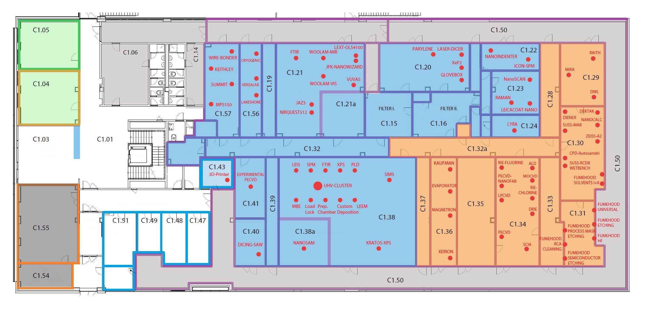
Floorplan and Equipment placement