
CEITEC Nano Research Infrastructure
Brno University of Technology
Purkyňova 123, 612 00 Brno
Czech Republic
 +420 54114 9207
 nano@ceitec.vutbr.cz
Consumables | ShP | today | feedback


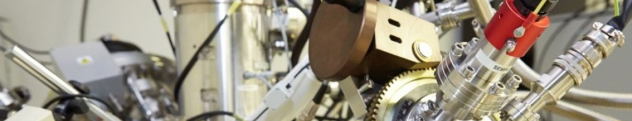
Scanning electron microscope (SEM) MIRA3 XMU (MIRA-STAN)

Guarantor:
Petr Lepcio, Ph.D.
Instrument status:
![]() Operational, 17.3.2026 11:17
Operational, 17.3.2026 11:17
Equipment placement:
CEITEC Nano - A1.11
Upcoming trainings:
29.7. 09:30 - 13:00:
MIRA-STAN 2/2 -
Meeting point at the microscope. This is a two-step training, register for part 1 in our booking system. More information about the training is available on our <a href=”https://cfmoodle.ceitec.vutbr.cz/course/view.php?id=76”>Moodle</a>.
22.7. 09:30 - 16:30:
MIRA-STAN 1/2 -
Meeting point at the microscope. This is a two-step training, register for part 2 in our booking system. Obligatory prerequisites must be completed 2 days before the training. More information about the training is available on our <a href=”https://cfmoodle.ceitec.vutbr.cz/course/view.php?id=76”>Moodle</a>.
Scanning electron microscope (SEM) MIRA3 XMU
Description
• Scanning electron microscope (SEM) is used to study the morphology and topography of conductive and non-conductive materials in high resolution (micro to nano-scale).
• Observation of surface samples with high depth of focus using multiple detection system (SE, BSE, STEM) including elemental analysis using energy dispersive spectrometer (EDS).
Applications
• Observation of both the surface and internal structure of micro and nano-objects (phase interface such as matrix-filler/reinforcement, particle distribution, aggregates and defects, fracture surfaces, porous 3D materials, units of supramolecular structure, etc.)
• evaluation of the shape and dimensions (length, diameter, volume, roughness) of powders, tubes, short fibers
• fast and highly accurate chemical microanalysis and elemental mapping of a sample surface
• qualitative elemental analysis including determination of the distribution of each element
• quantitative analysis of the individual elements in a sample
• The structural analysis of polymeric materials, biopolymers and composites, biomaterials, ceramics, bones, teeth, substrates for tissue engineering, etc.
Specification
• High Brightness Schottky Emitter
• Detectors:
SE, BSE, In-beam SE, In-Beam BSE
LVSTD
STEM detector
EDX analysis
• High-vacuum (≤9x10⁻³Pa) or low-vacuum mode (7-500 Pa)
• Magnification 25 to 1 000 000x
• Acceleration voltage 200 V to 30 kV
• X-Y-Z 130×130×100mm
• Maximum specimen height: 106 mm
Publications:
-
YOHANNAN, A.; VAGHASIYA, J.; SONIGARA, K.; PUMERA, M., 2026: Lunar regolith simulant-based triboelectric nanogenerators: Toward sustainable energy harvesting from resources on the moon. APPLIED MATERIALS TODAY , p. 1 - 9, doi: 10.1016/j.apmt.2025.103071; FULL TEXT
(MIRA-STAN, RIGAKU3) -
YOHANNAN, A.; SONIGARA, K.; VAGHASIYA, J.; PUMERA, M., 2026: Moon Regolith Simulant-Based All-3D-Printed Triboelectric Nanogenerator for Effective Mechanical Energy Conversion. ENERGY & FUELS , p. 3551 - 3561, doi: 10.1021/acs.energyfuels.5c04047; FULL TEXT
(MIRA-STAN, RIGAKU3) -
ŠIMŮNKOVÁ, H.; HRUSKA, M.; OTTA, J.; MISEK, J.; SMÍSITEL, P.; JANATA, M.; FITL, P.; VALLEJOS, S.; KOLÍBALOVÁ, E.; MATOLINOVA, I.; VOROCHTA, M.; VRNATA, M.; HUBÁLEK, J., 2026: Mechanistic insights into ethanol sensing by Pt-decorated WO3 nanowires. SENSORS AND ACTUATORS B-CHEMICAL 451, doi: 10.1016/j.snb.2025.139287; FULL TEXT
(TITAN, MIRA-STAN) -
JU, X.; VELLUVAKANDY, R.; WU, X.; MERLOS RODRIGO, M.; HEGER, Z.; BENDICKOVA, K.; FRIC, J.; PUMERA, M., 2026: Liquid Metal Microrobots for Magnetically Guided Transvascular Navigation. ADVANCED MATERIALS 18382, doi: 10.1002/adma.202518382; FULL TEXT
(MIRA-STAN, LYRA, RIGAKU3, VERSALAB, KRATOS-XPS) -
THEKKEDATH MADHU, N.; NATARAJAN, S.; PUMERA, M., 2026: Molecularly Engineered Fluorescent Magnetic Microrobots for Sensing High-Energy Nitroaromatic Explosives in Highly Acidic Aqueous Environments. SMALL 22(5), doi: 10.1002/smll.202512670; FULL TEXT
(JASCO, FTIR-CHEMLAB, LEICACOAT-STAN, VERIOS, MIRA-STAN)
-
CHENNAM, P.; ŘÍHOVÁ, M.; AZPEITIA, S.; SEPÚLVEDA SEPÚLVEDA, L.; KACHLÍK, M.; POUZAR, M.; CICMANCOVA, V.; MACA, K.; KNEZ, M.; MACÁK, J., 2026: Carbon fibers with infiltrated TiO2 nanocrystalline layers: photocatalytic performance. NANOSCALE 18(1), p. 413 - 424, doi: 10.1039/d5nr04109k; FULL TEXT
(VERIOS, RIGAKU3, MIRA-STAN, JASCO, WITEC-RAMAN, KRATOS-XPS) -
Joda, NN.; Edelmannova, MF.; Pavliñák, D.; Santana, VT.; Chennam, PK.; Rihova, M.; Kocí, K.; Macak, JM., 2025: Centrifugally spun hematite Fe2O3 hollow fibers: Efficient photocatalyst for H2 generation and CO2 reduction. APPLIED SURFACE SCIENCE 686, p. 1 - 12, doi: 10.1016/j.apsusc.2024.162132; FULL TEXT
(MIRA-STAN, LEICACOAT-STAN, RIGAKU3, WITEC-RAMAN, BET-DEGASSER, JASCO, KRATOS-XPS, BET-ANAMET) -
KOMÁRKOVÁ, M.; BENEŠÍK, M.; ČERNÁ, E.; SEDLÁČKOVÁ, L.; MOŠA, M.; VOJTOVÁ, L.; FRANC, A.; PANTŮČEK, R., 2025: The pharmaceutical quality of freeze-dried tablets containing therapeutic bacteriophages against Pseudomonas aeruginosa and Staphylococcus aureus. INTERNATIONAL JOURNAL OF PHARMACEUTICS 671, p. 1 - 9, doi: 10.1016/j.ijpharm.2025.125199; FULL TEXT
(MIRA-STAN, LEICACOAT-STAN) -
Nittoor-Veedu, R.; Ju, XH.; Langer, M.; Gao, WL.; Otyepka, M.; Pumera, M., 2025: Periodic Table Exploration of MXenes for Efficient Electrochemical Nitrate Reduction to Ammonia. SMALL 21(10), doi: 10.1002/smll.202410105; FULL TEXT
(MIRA-STAN, RIGAKU3, FTIR-CHEMLAB, KRATOS-XPS) -
Deshmukh, S.; Vaghasiya, JV.; Michalicka, J.; Langer, R.; Otyepka, M.; Pumera, M., 2025: Phase Transition Driven Zn-Ion Battery With Laser-Processed V2C/V2O5 Electrodes for Wearable Temperature Monitoring. SMALL 21(7), doi: 10.1002/smll.202409987; FULL TEXT
(TITAN, VERIOS, MIRA-STAN, WITEC-RAMAN, KRATOS-XPS) -
Alsoud, A.; Shaheen, AA.; Knápek, A.; Al-Bashaish, SR.; Ahmad, MDJ.; Mousa, MS.; Sobola, D., 2025: Fabrication and Electrical Characterization of Dot Capacitors for Cold Field Emission Applications. ACS OMEGA , p. 11108 - 11118, doi: 10.1021/acsomega.4c10081; FULL TEXT
(MIRA-STAN, IS-NOVOCONTROL) -
SONIGARA, K.; VAGHASIYA, J.; MAYORGA-MARTINEZ, C.; PUMERA, M.; , 2025: Point-of-use upcycling of 3D printing waste for developing 3D-printed Zn-I2 batteries. JOURNAL OF MATERIALS CHEMISTRY A 13(16), p. 11804 - 11816, doi: 10.1039/d5ta00919g; FULL TEXT
(WITEC-RAMAN, RIGAKU3, MIRA-STAN, KRATOS-XPS) -
Senthilnathan, N.; Oral, CM.; Pumera, M., 2025: Magneto-Fluorescent Microrobots with Selective Detection Intelligence for High-Energy Explosives and Antibiotics in Aqueous Environments. ACS APPLIED MATERIALS & INTERFACES , p. 21691 - 21704, doi: 10.1021/acsami.5c02259; FULL TEXT
(JASCO, FTIR-CHEMLAB, RIGAKU3, VERIOS, MIRA-STAN, LEICACOAT-STAN) -
Alsoud, A.; Al-Bashaish, SR.; Shaheen, AA.; Knápek, A.; Mousa, MS.; Sobola, D., 2025: Study of the dielectric properties, relaxation mechanisms and electrical conduction mechanisms of epoxy/ α-Iron oxide nanocomposites. JOURNAL OF ALLOYS AND COMPOUNDS 1022, doi: 10.1016/j.jallcom.2025.179806; FULL TEXT
(RIGAKU3, MIRA-STAN, FTIR, CITOPRESS, IS-NOVOCONTROL) -
STREĎANSKÁ, A.; ŠIMEK, M.; MATONOHOVÁ, J.; NEČAS, D.; VRBKA, M.; SUCHÁNEK, J.; PAVLIŇÁKOVÁ, V.; VOJTOVÁ, L.; HARTL, M.; KŘUPKA, I.; NEŠPOROVÁ, K., 2025: Optimizing Hyaluronan-Based Lubricants for Treating Thoracolumbar Fascia Pathologies: Insights from Tribological and Pharmacokinetic Studies. LUBRICANTS 13(4), p. 1 - 17, doi: 10.3390/lubricants13040184; FULL TEXT
(MIRA-STAN, LEICACOAT-STAN) -
Rihova, M.; Azpeitia, S.; Cihalova, K.; Michalicka, J.; Chennam, PK.; Kolibalova, E.; Svoboda, R.; Heger, Z.; Knez, M.; Macak, JM., 2025: Centrifugally spun and ZnO-infiltrated PVA fibers with antibacterial activity for treatment of Acne vulgaris. JOURNAL OF CONTROLLED RELEASE 383, p. 113777-1 - 113777-10, doi: 10.1016/j.jconrel.2025.113777; FULL TEXT
(MIRA-STAN, LEICACOAT-NANO, TITAN, RIGAKU3) -
ALSOUD, A.; SHAHEEN, A.; TOFEL, P.; KNÁPEK, A.; SOBOLA, D., 2025: Enhancing dielectric properties of epoxy-based nanocomposites reinforced with yttrium oxide (Y2O3) nanoparticles for high-voltage insulation. MATERIALS SCIENCE AND ENGINEERING B-ADVANCED FUNCTIONAL SOLID-STATE MATERIALS 320, doi: 10.1016/j.mseb.2025.118407; FULL TEXT
(RIGAKU3, MIRA-STAN, IS-NOVOCONTROL) -
Paul, D.; Humar, M.; Tesařová, D.; Petrič, M.; Gaff, M., 2025: Nanoparticle-based impregnation coatings for wood: improving hydrophobicity, mechanical properties, and blue stain fungi resistance through structure–property relationship. JOURNAL OF MATERIALS SCIENCE 60(31), doi: 10.1007/s10853-025-11247-0; FULL TEXT
(MIRA-STAN, LEICACOAT-STAN, FTIR-CHEMLAB) -
POLÁKOVÁ, V.; MATULOVÁ, J.; BRTNÍKOVÁ, J.; FOHLEROVÁ, Z.; ŠMERKOVÁ, K.; KAISER, J.; ZIKMUND, T.; PROCHÁZKOVÁ, P.; ŽÍDEK, J.; VOJTOVÁ, L., 2025: In Situ Homogeneous Generation of Copper Nanoparticles in Collagen-Cellulose Freeze-Dried Foams Using Natural Reduction Agents to Enhance Their Stability, Antibacterial Properties, and Cytocompatibility. ACS OMEGA 10(35), p. 39799 - 39813, doi: 10.1021/acsomega.5c03661; FULL TEXT
(MIRA-STAN, ZETASIZER, LEICACOAT-STAN, micro-CT-L240) -
WU, X.; PENG, X.; REN, L.; GUAN, J.; PUMERA, M., 2025: Reconfigurable Self-Assembling Photocatalytic Magnetic Liquid Metal Microrobot Swarm for Microplastic Capture and Degradation. SMALL 21(38), doi: 10.1002/smll.202501351; FULL TEXT
(MIRA-STAN, RIGAKU9, VERSALAB, KRATOS-XPS) -
KADLECOVA, Z.; CHAMRADOVA, I.; TUSLOVA, K.; REBENDA, D.; CIPEK, P.; GREGORA, J.; STREDANSKA, A.; SAWAE, Y.; MENCIK, P.; VRBKA, M.; VOJTOVÁ, L., 2025: Biomimetic pHEMA Hydrogels as an Alternative Cartilage-like Model Material for Biotribological Evaluations. ACS OMEGA 10(38), p. 44147 - 44161, doi: 10.1021/acsomega.5c05569; FULL TEXT
(MIRA-STAN, LEICACOAT-STAN, FTIR-CHEMLAB) -
Al-Bashaish, S. R., Shaheen, A. A., Assayed, G. A., Ababneh, E., Alsoud, A., Jaber, A. M., Abuamr, A.M., Al Dmour, H., Sobola,D. & Mousa, M. S., 2025: Synergistic effect of low-concentration carbon nanoparticles on enhancing dielectric and conductive properties of polyvinyl alcohol nanocomposites for high-performance electrolytes in solid-state batteries. MATERIALS SCIENCE AND ENGINEERING B-ADVANCED FUNCTIONAL SOLID-STATE MATERIALS 323, p. 118772 - , doi: 10.1016/j.mseb.2025.118772; FULL TEXT
(TGA-DISCOVERY, MIRA-STAN) -
SRODA, P.; PETKO, F.; SWIEZY, A.; LEPCIO, P.; GALEK, M.; FIEDOR, P.; SZYMASZEK, P.; TYSZKA-CZOCHARA, M.; ORTYL, J., 2025: High-Performance Thiadiazole Derivatives as a Nontoxic Components of Initiating Systems for the Obtaining of New Generation Composites. INDUSTRIAL & ENGINEERING CHEMISTRY RESEARCH 64(39), p. 19090 - 19107, doi: 10.1021/acs.iecr.5c02434; FULL TEXT
(MIRA-STAN) -
NITTOOR VEEDU, R.; KALLESHAPPA, B.; PUMERA, M., 2025: Copper-Infused MXene from MAX Phase for Enhanced Electrochemical Ammonia Production. ACS NANO 19(46), p. 39645 - 39653, doi: 10.1021/acsnano.5c09659; FULL TEXT
(MIRA-STAN, RIGAKU3, JASCO, KRATOS-XPS) -
Dumpíková, M.; Ivanova, A.; Kirchnerová, R.; Zikmundová, E.; Tuceková, ZK.; Pavlinák, D.; Kucková, S.; Vyskocilová, G., 2025: Complex Material Analysis of Reverse Painting on Glass by Means of Photography, Microscopy, and Spectroscopic Techniques. CHEMISTRY METHODS 5(10), p. 1 - 8, doi: 10.1002/cmtd.202500024; FULL TEXT
(MIRA-STAN, FTIR-CHEMLAB) -
Kipkurui Ronoh; Ivo Šulák; Dinara Sobola, 2025: Effect of ultrafast laser ablation on the wettability of superalloys. PROCEDIA STRUCTURAL INTEGRITY 74, p. 77 - 84, doi: 10.1016/j.prostr.2025.10.037; FULL TEXT
(VERIOS, MIRA-STAN, DEKTAK, SEE-SYSTEM, KRATOS-XPS) -
NGHIEM, X.; BIRGUSOVÁ, E.; PEKÁRKOVÁ, J.; BYTEŠNÍKOVÁ, Z.; RICHTERA, L., 2025: INVESTIGATING THE IMPACT OF SYNTHESIS PROCEDURES ON ELECTROCHEMICAL PROPERTIES OF rGO-CeO2 NANOCOMPOSITE. NANOCON CONFERENCE PROCEEDINGS - INTERNATIONAL CONFERENCE ON NANOMATERIALS (1), p. 47 - 52, doi: 10.37904/nanocon.2024.4994
(MIRA-STAN) -
PENG, X.; ORAL, Ç.; URSO, M.; USSIA, M.; PUMERA, M., 2025: Active Microrobots for Dual Removal of Biofilms via Chemical and Physical Mechanisms. ACS APPLIED MATERIALS & INTERFACES , p. 3608 - 3619, doi: 10.1021/acsami.4c18360; FULL TEXT
(VERSALAB, KRATOS-XPS, MIRA-STAN) -
RONOH, K.; NOVOTNÝ, J.; MRŇA, L.; KNÁPEK, A.; SOBOLA, D., 2024: Analysis of processing efficiency, surface, and bulk chemistry, and nanomechanical properties of the Monel® alloy 400 after ultrashort pulsed laser ablation. MATERIALS RESEARCH EXPRESS 11(1), doi: 10.1088/2053-1591/ad184b; FULL TEXT
(DEKTAK, MIRA-STAN, NANOINDENTER, KRATOS-XPS) -
DRDLÍK, D.; MAŘÁK, V.; HADRABA, H.; CHLUP, Z., 2024: A way for densification of lead-free BaTiO3-based/ZrO2 laminates for energy harvesting applications prepared by electrophoretic deposition. MATERIALS LETTERS 335, doi: 10.1016/j.matlet.2023.135424; FULL TEXT
(MIRA-STAN) -
RONOH, K.; NOVOTNÝ, J.; MRŇA, L.; KNÁPEK, A.; SOBOLA, D., 2024: Surface Structuring of the CP Titanium by Ultrafast Laser Pulses. MATERIALS RESEARCH EXPRESS 14(8), p. 1 - 21, doi: 10.3390/app14083164; FULL TEXT
(MIRA-STAN, WITEC-RAMAN, SEE-SYSTEM, DEKTAK) -
VELIKOV, D.; JANČÍK PROCHÁZKOVÁ, A.; PUMERA, M., 2024: On-the-Fly Monitoring of the Capture and Removal of Nanoplastics with Nanorobots. ACS NANOSCIENCE AU 4(4), p. 243 - 7, doi: 10.1021/acsnanoscienceau.4c00002; FULL TEXT
(MIRA-STAN) -
VALÁŠEK, D.; POUCHLÝ, V.; SALAMON, D., 2024: Turning of high entropy alloy into high entropy carbides by modifying carbon content during reactive sintering. CERAMICS INTERNATIONAL 50(9), p. 15367 - 6, doi: 10.1016/j.ceramint.2024.01.438; FULL TEXT
(MIRA-STAN, RIGAKU3) -
USSIA, M.; URSO, M.; ORAL, Ç.; PENG, X.; PUMERA, M., 2024: Magnetic Microrobot Swarms with Polymeric Hands Catching Bacteria and Microplastics in Water. ACS NANO (E-ISSN) 18(20), p. 13171 - 13, doi: 10.1021/acsnano.4c02115; FULL TEXT
(MIRA-STAN) -
NATARAJAN, S.; ORAL, Ç.; NOVOBILSKÝ, A.; PUMERA, M., 2024: Intelligent Magnetic Microrobots with Fluorescent Internal Memory for Monitoring Intragastric Acidity. ADVANCED FUNCTIONAL MATERIALS 34(29), p. 1 - 12, doi: 10.1002/adfm.202401463; FULL TEXT
(FTIR-CHEMLAB, VERIOS, MIRA-STAN, LEICACOAT-STAN, RIGAKU3) -
Gazdík, R., 2024: Defect localization and analysis in GaN. MASTER´S THESIS , p. 1 - 66; FULL TEXT
(MIRA-STAN, HELIOS, TITAN) -
KORČUŠKOVÁ, M.; SVATÍK, J.; TOMAL, W.; ŠIKYŇOVÁ, A.; VISHAKHA, V.; PETKO, F.; GALEK, M.; STALMACH, P.; ORTYL, J.; LEPCIO, P., 2024: Anatase and rutile nanoparticles in photopolymer 3D-printed nanocomposites: Band gap-controlled electron interactions in free-radical and cationic photocuring. REACTIVE & FUNCTIONAL POLYMERS 200, p. 1 - 12, doi: 10.1016/j.reactfunctpolym.2024.105923; FULL TEXT
(WITEC-RAMAN, JASCO, MIRA-STAN, DSC-DISCOVERY) -
Escalera-López, D.; Iffelsberger, C.; Zlatar, M.; Novcic, K.; Maselj, N.; Van Pham, C.; Jovanovic, P.; Hodnik, N.; Thiele, S.; Pumera, M.; Cherevko, S. , 2024: Allotrope-dependent activity-stability relationships of molybdenum sulfide hydrogen evolution electrocatalysts. NATURE COMMUNICATIONS 15(1), doi: 10.1038/s41467-024-47524-w; FULL TEXT
(MIRA-STAN, WITEC-RAMAN, KRATOS-XPS) -
HOLÁ, M.; SALAJKOVÁ, Z.; GREGAR, F.; ONDRÁČEK, J.; PAVLIŇÁK, D.; ŠPERKA, P.; HRDLIČKA, A.; KAISER, J.; KANICKÝ, V., 2024: Laser spot overlap in scanning laser ablation ICP-MS analysis: Impact on analytical signal and properties of the generated aerosol. SPECTROCHIMICA ACTA PART B-ATOMIC SPECTROSCOPY 219, doi: 10.1016/j.sab.2024.106999; FULL TEXT
(MIRA-STAN) -
JANČÍK PROCHÁZKOVÁ, A.; JANČÍK, J.; PALACIOS CORELLA, M.; PUMERA, M., 2024: Microrobots Enhancing Synthetic Chemistry Reactions in Non-Aqueous Media. ADVANCED FUNCTIONAL MATERIALS 34(49), doi: 10.1002/adfm.202409459; FULL TEXT
(MIRA-STAN, LEICACOAT-STAN, RIGAKU3, KRATOS-XPS) -
HÜLAGÜ, D.; TOBIAS, C.; DAO, R.; KOMAROV, P.; RURACK, K.; HODOROABA, V., 2024: Towards 3D determination of the surface roughness of core-shell microparticles as a routine quality control procedure by scanning electron microscopy. SCIENTIFIC REPORTS 14(1), p. 1 - 13, doi: 10.1038/s41598-024-68797-7; FULL TEXT
(LITESCOPE-MIRA-STAN, MIRA-STAN) -
ALLAHAM, M.; DARADKEH, S.; AL-BRAIKAT, H.; DALLAEV, R.; BURDA, D.; KOŠELOVÁ, Z.; AL-AKHRAS, M.; JABER, A.; MOUSA, M.; SOBOLA, D.; KOLAŘÍK, V.; KNÁPEK, A., 2024: Comprehensive analysis of charge carriers dynamics through the honeycomb structure of graphite thin films and polymer graphite with applications in cold field emission and scanning tunneling microscopy. SURFACES AND INTERFACES 53, p. 1 - 15, doi: 10.1016/j.surfin.2024.105102; FULL TEXT
(MIRA-STAN, KRATOS-XPS) -
NASERI JODA, N.; INCE, A.; ŘÍHOVÁ, M.; PAVLIŇÁK, D.; MACÁK, J., 2024: Design of collectors in centrifugal spinning: Effect on the fiber yield and morphology. JOURNAL OF INDUSTRIAL TEXTILES 54, p. 1 - 20, doi: 10.1177/15280837241298641; FULL TEXT
(MIRA-STAN, LEICACOAT-STAN) -
ALSOUD, A.; DARADKEH, S.; SHAHEEN, A.; AL-HROUB, Q.; KNÁPEK, A.; MOUSA, M.; SOBOLA, D., 2024: Electrical properties of epoxy/graphite flakes microcomposite at the percolation threshold concentration. PHYSICA SCRIPTA 99(5), p. 1 - 15, doi: 10.1088/1402-4896/ad3b50; FULL TEXT
(MIRA-STAN, JAZ3-CHANNEL, FTIR, KRATOS-XPS) -
ŘÍHOVÁ, M.; ČÍHALOVÁ, K.; POUZAR, M.; KUTHANOVÁ, M.; JELÍNEK, L.; HROMÁDKO, L.; ČIČMANCOVÁ, V.; HEGER, Z.; MACÁK, J., 2024: Biopolymeric fibers prepared by centrifugal spinning blended with ZnO nanoparticles for the treatment of Acne vulgaris. APPLIED MATERIALS TODAY 37, doi: 10.1016/j.apmt.2024.102151; FULL TEXT
(TITAN, MIRA-STAN) -
RONOH, K.; NOVOTNÝ, J.; MRŇA, L.; KNÁPEK, A.; SOBOLA, D., 2024: Ablation characteristics of the nickel-based superalloy, 699 XA using ultrafast laser. APPLIED SURFACE SCIENCE , doi: 10.1016/j.apsusc.2024.161687; FULL TEXT
(WITEC-RAMAN, VERIOS, MIRA-STAN, DEKTAK, KRATOS-XPS) -
Assayed, GAI.; Shaheen, AA.; Alsoud, A.; Al-Bashaish, SR.; Mousa, MS.; Knapek, A.; Sobola, D., 2024: Structural and electrical characterization of cadmium phosphate glasses doped with different concentration of sodium chloride. PHYSICA SCRIPTA 99(12), doi: 10.1088/1402-4896/ad8822; FULL TEXT
(RIGAKU3, FTIR, MIRA-STAN, IS-NOVOCONTROL) -
Očkovič, A., 2024: In-situ characterization of semiconductors using scanning probe microscopy techniques. MASTER´S THESIS , p. 1 - 74; FULL TEXT
(LITESCOPE-MIRA-STAN, MIRA-STAN) -
UKROPCOVÁ, I.; DAO, R.; ŠTUBIAN, M.; KOLÍBAL, M.; ŠIKOLA, T.; WILLINGER, M.; WANG, Z.; ZLÁMAL, J.; BÁBOR, P., 2023: Electron Tractor Beam: Deterministic Manipulation of Liquid Droplets on Solid Surfaces. ADVANCED MATERIALS INTERFACES 10(2), doi: 10.1002/admi.202201963; FULL TEXT
(NANOSAM, LITESCOPE-LYRA, MIRA-STAN) -
ŠKARPA, P.; JANČÁŘ, J.; LEPCIO, P.; ANTOŠOVSKÝ, J.; KLOFÁČ, D.; KRIŠKA, T.; ABDELLATIF, A.; BRTNICKÝ, M., 2023: Effect of fertilizers enriched with bio-based carriers on selected growth parameters, grain yield and grain quality of maize (Zea mays L.) . EUROPEAN JOURNAL OF AGRONOMY 143, doi: 10.1016/j.eja.2022.126714; FULL TEXT
(FTIR-CHEMLAB, MIRA-STAN) -
SLÁMEČKA, K.; KASHIMBETOVA, A.; POKLUDA, J.; ZIKMUND, T.; KAISER, J.; MONTUFAR JIMENEZ, E.; ČELKO, L., 2023: Fatigue behaviour of titanium scaffolds with hierarchical porosity produced by material extrusion additive manufacturing. MATERIALS & DESIGN 225, p. 1 - 11, doi: 10.1016/j.matdes.2022.111453; FULL TEXT
(MIRA-STAN, micro-CT-L240, RIGAKU3) -
Jancik-Prochazkova, A.; Michalkova, H.; Heger, Z.; Pumera, M., 2023: Hydrogen Bonding Nanoarchitectonics of Organic Pigment-Based Janus Microrobots with Entering Capability into Cancer Cells. ACS NANO 17(1), p. 146 - 156, doi: 10.1021/acsnano.2c05585; FULL TEXT
(VERIOS, MIRA-STAN, LEICACOAT-STAN, FTIR) -
SANNA, M.; NOVCIC, K.; NG, S.; ČERNÝ, M.; PUMERA, M., 2023: The unexpected photoelectrochemical activity of MAX phases: the role of oxide impurities. JOURNAL OF MATERIALS CHEMISTRY A 11(6), p. 3080 - 11, doi: 10.1039/d2ta06929f; FULL TEXT
(MIRA-STAN, RIGAKU3, KRATOS-XPS) -
USSIA, M.; URSO, M.; KRATOCHVÍLOVÁ, M.; NAVRÁTIL, J.; BALVAN, J.; MAYORGA-MARTINEZ, C.; VYSKOČIL, J.; MASAŘÍK, M.; PUMERA, M., 2023: Magnetically Driven Self-Degrading Zinc-Containing Cystine Microrobots for Treatment of Prostate Cancer. SMALL 19(17), doi: 10.1002/smll.202208259; FULL TEXT
(MIRA-STAN) -
ORAL, Ç.; USSIA, M.; URSO, M.; SALÁT, J.; NOVOBILSKÝ, A.; ŠTEFÁNIK, M.; RŮŽEK, D.; PUMERA, M., 2023: Radiopaque Nanorobots as Magnetically Navigable Contrast Agents for Localized In Vivo Imaging of the Gastrointestinal Tract. ADVANCED HEALTHCARE MATERIALS 12(8), doi: 10.1002/adhm.202202682; FULL TEXT
(VERIOS, MIRA-STAN, RIGAKU3, VERSALAB) -
RYŠAVÁ, L.; DVOŘÁK, M.; VOJTOVÁ, L.; DORAZILOVÁ, J.; SEDLÁČEK, P.; KUBÁŇ, P., 2023: Fully soluble polymeric foams for in-vial dried blood spot collection and analysis of acidic drugs by capillary electrophoresis. ANALYTICA CHIMICA ACTA 1241, doi: 10.1016/j.aca.2023.340793; FULL TEXT
(MIRA-STAN) -
Gustafsson, L.; Kvick, M.; Åstrand, C.; Ponsteen, N.; Dorka, N.; Hegrová, V.; Svanberg, S.; Horák, J.; Jansson, R.; Hedhammar, M.; van der Wijngaart, W., 2023: Scalable Production of Monodisperse Bioactive Spider Silk Nanowires. MACROMOLECULAR BIOSCIENCE 23(4), doi: 10.1002/mabi.202200450; FULL TEXT
(MIRA-STAN) -
GHOSH, K.; IFFELSBERGER, C.; KONEČNÝ, M.; VYSKOČIL, J.; MICHALIČKA, J.; PUMERA, M., 2023: Nanoarchitectonics of Triboelectric Nanogenerator for Conversion of Abundant Mechanical Energy to Green Hydrogen. ADVANCED ENERGY MATERIALS 13(11), doi: 10.1002/aenm.202203476; FULL TEXT
(VERIOS, MIRA-STAN, TITAN, RIGAKU3, MPS150, KEITHLEY-4200, ICON-SPM) -
PENG, X.; URSO, M.; PUMERA, M., 2023: Metal oxide single-component light-powered micromotors for photocatalytic degradation of nitroaromatic pollutants. NPJ CLEAN WATER 6(6), p. 1 - 7, doi: 10.1038/s41545-023-00235-z; FULL TEXT
(MIRA-STAN, KRATOS-XPS) -
JANČÍK PROCHÁZKOVÁ, A.; PUMERA, M., 2023: Light-powered swarming phoretic antimony chalcogenide-based microrobots with ´on-the-fly´ photodegradation abilities. NANOSCALE 15(12), p. 5726 - 9, doi: 10.1039/d3nr00098b; FULL TEXT
(MIRA-STAN, RIGAKU3) -
JANČÍK PROCHÁZKOVÁ, A.; JAŠEK, V.; FIGALLA, S.; PUMERA, M., 2023: Photocatalytic Microplastics ´On-The-fly´ Degradation via Motile Quantum Materials-Based Microrobots. ADVANCED OPTICAL MATERIALS , p. 1 - 9, doi: 10.1002/adom.202300782; FULL TEXT
(MIRA-STAN, RIGAKU3) -
TINOCO NAVARRO, L.; BEDNAŘÍKOVÁ, V.; KAŠTYL, J.; CIHLÁŘ, J., 2023: Structure and Photocatalytic Properties of Ni-, Co-, Cu-, and Fe-Doped TiO2 Aerogels. GELS 9(5), p. 1 - 21, doi: 10.3390/gels9050357; FULL TEXT
(RIGAKU3, VERIOS, JASCO, MIRA-STAN, TITAN, BET-ANAMET) -
Žůrek, M., 2023: Butyl Rubber Modified Using Expanded Graphite. MASTER´S THESIS ; FULL TEXT
(MIRA-STAN) -
Novotný, K., 2023: Composite materials with enhanced coefficient of linear attenuation of ionizing radiation. MASTER´S THESIS ; FULL TEXT
(MIRA-STAN) -
KACVINSKÁ, K.; PAVLIŇÁKOVÁ, V.; POLÁČEK, P.; MICHLOVSKÁ, L.; HEFKA BLAHNOVÁ, V.; FILOVÁ, E.; KNOZ, M.; LIPOVÝ, B.; HOLOUBEK, J.; FALDYNA, M.; PAVLOVSKÝ, Z.; VÍCENOVÁ, M.; CVANOVÁ, M.; JARKOVSKÝ, J.; VOJTOVÁ, L., 2023: Accelular nanofbrous bilayer scafold intrapenetrated with polydopamine network and implemented into a full-thickness wound of a white-pig model afects infammation and healing process. JOURNAL OF NANOBIOTECHNOLOGY 21(1), p. 1 - 24, doi: 10.1186/s12951-023-01822-5; FULL TEXT
(MIRA-STAN) -
Bondarev, A.; Simonovic, K.; Vitu, T.; Kožmín, P.; Syrovatka, Š.; Polcar, T., 2023: Textured coating or coated texture: Femtosecond laser texturing of a-C:H/WC coatings for dry friction applications. SURFACE AND COATINGS TECHNOLOGY 469, doi: 10.1016/j.surfcoat.2023.129808; FULL TEXT
(HELIOS, MIRA-STAN, KRATOS-XPS) -
JAQUES, V.; HOLCOVÁ, K., 2023: Calcareous nannofossil assemblage in paintings chalk ground for provenance analysis: three original paintings compared to european source materials. HERITAGE SCIENCE 11(1), p. 1 - 11, doi: 10.1186/s40494-023-00974-9; FULL TEXT
(MIRA-STAN) -
DEÁK, A.; SZABÓ, P.; BEDNAŘÍKOVÁ, V.; CIHLÁŘ, J.; DEMETER, A.; REMEŠOVÁ, M.; COLACINO, E.; ČELKO, L., 2023: The first solid-state route to luminescent Au(I)-glutathionate and its pH-controlled transformation into ultrasmall oligomeric Au10-12(SG)10-12 nanoclusters for application in cancer radiotheraphy. FRONTIERS IN CHEMISTRY 11, doi: 10.3389/fchem.2023.1178225; FULL TEXT
(RIGAKU3, MIRA-STAN, VERIOS, LEICACOAT-STAN, KRATOS-XPS) -
SEDLÁŘ, M.; VERČIMÁKOVÁ, K.; FOHLEROVÁ, Z.; IZSÁK, D.; CHALUPOVÁ, M.; SUCHÝ, P.; DOHNALOVÁ, M.; SOPUCH, T.; VOJTOVÁ, L., 2023: A synergistic effect of fibrous carboxymethyl cellulose with equine collagen improved the hemostatic properties of freeze-dried wound dressings. CELLULOSE , p. 1 - 19, doi: 10.1007/s10570-023-05571-4; FULL TEXT
(LEICACOAT-STAN, MIRA-STAN) -
Vida, J.; Pospisil, J.; Souček, P.; Weiter, M.; Homola, T., 2023: Rapid, low-temperature, air plasma sintering of mesoporous titania electron transporting layers in perovskite solar cells. SOLAR ENERGY MATERIALS AND SOLAR CELLS 263, doi: 10.1016/j.solmat.2023.112562; FULL TEXT
(MIRA-STAN, KRATOS-XPS) -
SEVRIUGINA, V.; PAVLIŇÁK, D.; ONDREÁŠ, F.; JAŠEK, O.; ŠTAFFOVÁ, M.; LEPCIO, P., 2023: Matching Low Viscosity with Enhanced Conductivity in Vat Photopolymerization 3D Printing: Disparity in the Electric and Rheological Percolation Thresholds of Carbon-Based Nanofillers Is Controlled by the Matrix Type and Filler Dispersion. ACS OMEGA 8(48), p. 45566 - 12, doi: 10.1021/acsomega.3c05683; FULL TEXT
(WITEC-RAMAN, BET-DEGASSER, MIRA-STAN, FTIR-CHEMLAB, LEICACOAT-STAN, DHR, KRATOS-XPS) -
WERT, S.; IFFELSBERGER, C.; KANDAMBATH PADINJAREVEETIL, A.; PUMERA, M., 2023: Edges of Layered FePSe3 Exhibit Increased Electrochemical and Electrocatalytic Activity Compared to Basal Planes. ACS APPLIED ELECTRONIC MATERIALS 5(2), p. 928 - 7, doi: 10.1021/acsaelm.2c01493; FULL TEXT
(RIGAKU3, MIRA-STAN) -
VISHAKHA, V.; ABDELLATIF, A.; MICHALIČKA, J.; WHITE, P.; LEPCIO, P.; TINOCO NAVARRO, L.; JANČÁŘ, J., 2023: Carboxymethyl starch as a reducing and capping agent in the hydrothermal synthesis of selenium nanostructures for use with three-dimensional-printed hydrogel carriers. ROYAL SOCIETY OPEN SCIENCE 10(10), p. 1 - 17, doi: 10.1098/rsos.230829; FULL TEXT
(ZETASIZER, RIGAKU3, VERIOS, MIRA-STAN, LEICACOAT-STAN, TITAN, FTIR-CHEMLAB, JASCO, KRATOS-XPS) -
KADLECOVÁ, Z.; SEVRIUGINA, V.; LYSÁKOVÁ, K.; RYCHETSKÝ, M.; CHAMRADOVÁ, I.; VOJTOVÁ, L., 2023: Liposomes Affect Protein Release and Stability of ITA-Modified PLGA-PEG-PLGA Hydrogel Carriers for Controlled Drug Delivery. BIOMACROMOLECULES 25(1), p. 67 - 10, doi: 10.1021/acs.biomac.3c00736; FULL TEXT
(DAWN-HELEOS, ZETASIZER, NMR, MIRA-STAN) -
TESAŘ, J.; MUNOZ MARTIN, J.; PUMERA, M., 2022: Limitations and Benefits of MAX Phases in Electroanalysis. ELECTROANALYSIS 33, p. 56 - 5, doi: 10.1002/elan.202100473; FULL TEXT
(MIRA-STAN) -
GAO, W.; MICHALIČKA, J.; PUMERA, M., 2022: Hierarchical Atomic Layer Deposited V2O5 on 3D Printed Nanocarbon Electrodes for High-Performance Aqueous Zinc-Ion Batteries. SMALL 18(1), p. 2105572-1 - 13, doi: 10.1002/smll.202105572; FULL TEXT
(ALD-FIJI, VERIOS, MIRA-STAN, TITAN, RIGAKU3, KRATOS-XPS) -
MAYORGA BURREZO, P.; MAYORGA-MARTINEZ, C.; PUMERA, M., 2022: Light-Driven Micromotors to Dissociate Protein Aggregates That Cause Neurodegenerative Diseases. ADVANCED FUNCTIONAL MATERIALS , p. 2106699-1 - 8, doi: 10.1002/adfm.202106699; FULL TEXT
(MIRA-STAN, RIGAKU9, KRATOS-XPS) -
NOVCIC, K.; IFFELSBERGER, C.; PUMERA, M., 2022: Layered MAX phase electrocatalyst activity is driven by only a few hot spots. JOURNAL OF MATERIALS CHEMISTRY A , p. 3206 - 10, doi: 10.1039/d1ta06419c; FULL TEXT
(RIGAKU9, MIRA-STAN, LEICACOAT-STAN, ICON-SPM) -
WERT, S.; IFFELSBERGER, C.; NOVCIC, K.; MATYSIK, F.; PUMERA, M., 2022: Edges are more electroactive than basal planes in synthetic bulk crystals of TiS2 and TiSe2. APPLIED MATERIALS TODAY 26, p. 101309-1 - 7, doi: 10.1016/j.apmt.2021.101309; FULL TEXT
(MIRA-STAN, ICON-SPM, KRATOS-XPS) -
ORAL, Ç.; USSIA, M.; YAVUZ, D.; PUMERA, M., 2022: Shape Engineering of TiO2 Microrobots for ´On-the-Fly´ Optical Brake. SMALL 18(10), p. 21076271-6 - 6, doi: 10.1002/smll.202106271; FULL TEXT
(LEICACOAT-STAN, VERIOS, MIRA-STAN, RIGAKU3) -
MUNOZ MARTIN, J.; URSO, M.; PUMERA, M., 2022: Self-Propelled Multifunctional Microrobots Harboring Chiral Supramolecular Selectors for ´Enantiorecogniton-on-the-Fly´. ANGEWANDTE CHEMIE-INTERNATIONAL EDITION 61(14), p. 1 - 7, doi: 10.1002/anie.202116090; FULL TEXT
(MIRA-STAN, VERSALAB) -
LEPCIO, P.; SVATÍK, J.; REŽNÁKOVÁ, E.; ZICHA, D.; LESSER, A.; ONDREÁŠ, F., 2022: Anisotropic solid-state PLA foaming templated by crystal phase pre-oriented with 3D printing: cell supporting structures with directional capillary transfer function. JOURNAL OF MATERIALS CHEMISTRY B 10(15), p. 2889 - 10, doi: 10.1039/d1tb02133h; FULL TEXT
(MIRA-STAN, FTIR-CHEMLAB, LEICACOAT-STAN) -
USSIA, M.; URSO, M.; KMENT, Š.; FIALOVÁ, T.; KLÍMA, K.; DOLEŽELÍKOVÁ, K.; PUMERA, M., 2022: Light-Propelled Nanorobots for Facial Titanium Implants Biofilms Removal. SMALL 18(22), p. 1 - 10, doi: 10.1002/smll.202200708; FULL TEXT
(MIRA-STAN, LEICACOAT-STAN) -
PENG, X.; URSO, M.; USSIA, M.; PUMERA, M., 2022: Shape-Controlled Self-Assembly of Light-Powered Microrobots into Ordered Microchains for Cells Transport and Water Remediation. ACS NANO 16(5), p. 7615 - 11, doi: 10.1021/acsnano.1c11136; FULL TEXT
(MIRA-STAN, RIGAKU3) -
IFFELSBERGER, C.; ROJAS TIZÓN, J.; PUMERA, M., 2022: Photo-Responsive Doped 3D-Printed Copper Electrodes for Water Splitting: Refractory One-Pot Doping Dramatically Enhances the Performance. JOURNAL OF PHYSICAL CHEMISTRY C (WEB) 126(21), p. 9016 - 11, doi: 10.1021/acs.jpcc.1c10686; FULL TEXT
(TEGRAMIN, MIRA-STAN, RIGAKU3, KRATOS-XPS) -
MUNOZ MARTIN, J.; IFFELSBERGER, C.; REDONDO NEGRETE, E.; PUMERA, M., 2022: Design of bimetallic 3D-printed electrocatalysts via galvanic replacement to enhance energy conversion systems. APPLIED CATALYSIS B: ENVIRONMENTAL 316, p. 1 - 9, doi: 10.1016/j.apcatb.2022.121609; FULL TEXT
(TEGRAMIN, CITOVAC, MIRA-STAN, RIGAKU9, KRATOS-XPS) -
IFFELSBERGER, C.; NG, S.; PUMERA, M., 2022: Photoelectrolysis of TiO2 is highly localized and the selectivity is affected by the light. CHEMICAL ENGINEERING JOURNAL 446, p. 136995-1 - 12, doi: 10.1016/j.cej.2022.136995; FULL TEXT
(WITEC-RAMAN, VERIOS, MIRA-STAN, RIGAKU3, KRATOS-XPS) -
Čermák, A.; Simonović, K.; Bondarev, A.; Kožmín, P.; Syrovátka, Š.; Polcar, T.; Syrovátka, J., 2022: Femtosecond laser texturing of DLC-based coatings by DLW method with sub-micrometer precision. THE INTERNATIONAL JOURNAL OF ADVANCED MANUFACTURING TECHNOLOGY 121(11-12), p. 8479 - 8494, doi: 10.1007/s00170-022-09855-0; FULL TEXT
(MIRA-STAN, KRATOS-XPS) -
KORČUŠKOVÁ, M.; SEVRIUGINA, V.; ONDREÁŠ, F.; SVATÍK, J.; TOMAL, W.; VISHAKHA, V.; ORTYL, J.; LEPCIO, P., 2022: Photoactivity, conversion kinetics, nanoreinforcement, post-curing, and electric/dielectric properties of functional 3D printable photopolymer resin filled with bare and alumina-doped ZnO nanoparticles. POLYMER TESTING 116, p. 1 - 10, doi: 10.1016/j.polymertesting.2022.107798; FULL TEXT
(MIRA-STAN, FTIR-CHEMLAB, RIGAKU9, DSC-DISCOVERY) -
ŠTAFFOVÁ, M.; ONDREÁŠ, F.; SVATÍK, J.; ZBONČÁK, M.; JANČÁŘ, J.; LEPCIO, P., 2022: 3D printing and post-curing optimization of photopolymerized structures: Basic concepts and effective tools for improved thermomechanical properties. POLYMER TESTING 108, p. 1 - 11, doi: 10.1016/j.polymertesting.2022.107499; FULL TEXT
(FTIR-CHEMLAB, MIRA-STAN, LEICACOAT-STAN, LEXT, RSA) -
ŘÍHOVÁ, M.; LEPCIO, P.; ČIČMANCOVÁ, V.; FRUMAROVÁ, B.; HROMÁDKO, L.; BUREŠ, F.; VOJTOVÁ, L.; MACÁK, J., 2022: The centrifugal spinning of vitamin doped natural gum fibers for skin regeneration. CARBOHYDRATE POLYMERS (ELECTRONIC) 294, p. 1 - 10, doi: 10.1016/j.carbpol.2022.119792; FULL TEXT
(MIRA-STAN, FTIR-CHEMLAB, LEICACOAT-STAN, IR-RAMAN) -
LEPCIO, P.; SVATÍK, J.; ŠTAFFOVÁ, M.; LESSER, A.; ONDREÁŠ, F., 2022: Revealing the Combined Nanoconfinement Effect by Soft and Stiff Inclusions in PMMA/Silica CO2 Blown Foams. MACROMOLECULAR MATERIALS AND ENGINEERING 307(11), p. 1 - 9, doi: 10.1002/mame.202200403; FULL TEXT
(MIRA-STAN, LEICACOAT-STAN, FTIR-CHEMLAB) -
MUNOZ MARTIN, J.; ROJAS TIZÓN, J.; PUMERA, M., 2022: Faceted Crystal Nanoarchitectonics of Organic-Inorganic 3D-Printed Visible-Light Photocatalysts. ACS APPLIED ENERGY MATERIALS 5(3), p. 3252 - 7, doi: 10.1021/acsaem.1c03863; FULL TEXT
(MIRA-STAN, KRATOS-XPS) -
URSO, M.; USSIA, M.; NOVOTNÝ, F.; PUMERA, M., 2022: Trapping and detecting nanoplastics by MXene-derived oxide microrobots. NATURE COMMUNICATIONS 13(1), p. 3573-1 - 14, doi: 10.1038/s41467-022-31161-2; FULL TEXT
(LEICACOAT-NANO, MIRA-STAN, RIGAKU9, VERSALAB, KRATOS-XPS) -
KANDAMBATH PADINJAREVEETIL, A.; ALDUHAISH, O.; ADIL, S.; PUMERA, M., 2022: Grafting of Pd on Covalently and Noncovalently Modified N-Doped Graphene for Electrocatalysis. ADVANCED MATERIALS INTERFACES 9(27), p. 2102317 - 8, doi: 10.1002/admi.202102317; FULL TEXT
(MIRA-STAN, LYRA, KRATOS-XPS) -
MILOSAVLJEVIĆ, V.; KOŠARIŠŤANOVÁ, L.; DOLEŽELÍKOVÁ, K.; ADAM, V.; PUMERA, M., 2022: Microrobots with Antimicrobial Peptide Nanoarchitectonics for the Eradication of Antibiotic-Resistant Biofilms. ADVANCED MATERIALS FOR OPTICS AND ELECTRONICS 32(43), p. 1 - 11, doi: 10.1002/adfm.202112935; FULL TEXT
(LEICACOAT-NANO, MIRA-EBL, MIRA-STAN, KRATOS-XPS) -
Jancik-Prochazkova, A.; Mayorga-Martinez, C. C.; Vyskočil, J.; Pumera, M., 2022: Swarming Magnetically Navigated Indigo-Based Hydrophobic Microrobots for Oil Removal. ACS APPLIED MATERIALS & INTERFACES 14(40), p. 45545 - 45552, doi: 10.1021/acsami.2c09527; FULL TEXT
(LEICACOAT-NANO, MIRA-STAN, FTIR) -
PENG, X.; URSO, M.; BALVAN, J.; MASAŘÍK, M.; PUMERA, M., 2022: Self-Propelled Magnetic Dendrite-Shaped Microrobots for Photodynamic Prostate Cancer Therapy. ANGEWANDTE CHEMIE-INTERNATIONAL EDITION 61(48), doi: 10.1002/anie.202213505; FULL TEXT
(MIRA-STAN, RIGAKU3, KRATOS-XPS) -
Breuer, JP.; Galgoczi, G.; Fioretti, V.; Zlamal, J.; Liska, P.; Werner, N.; Santin, G.; Boudin, N.; Ferreira, I. ; Guainazzi, M.; von Kienlin, A. ; Lotti, S.; Mineo, T.; Molendi, S.; Perinati, E., 2022: Athena charged particle diverter simulations: effects of micro-roughness on proton scattering using Geant4. SPACE TELESCOPES AND INSTRUMENTATION 2022: ULTRAVIOLET TO GAMMA RAY , doi: 10.1117/12.2630076; FULL TEXT
(MIRA-STAN, ICON-SPM) -
BÁČOVÁ, J.; HROMÁDKO, L.; NÝVLTOVÁ, P.; BRŮČKOVÁ, L.; MOTOLA, M.; BULÁNEK, R.; ŘÍHOVÁ, M.; ROUŠAR, T.; MACÁK, J., 2022: Ceramic fibers do not exhibit larger toxicity in pulmonary epithelial cells than nanoparticles of the same chemical composition. ENVIRONMENTAL SCIENCE: NANO 9(12), p. 4484 - 13, doi: 10.1039/d2en00217e; FULL TEXT
(MIRA-STAN) -
JAQUES, V.; ZIKMUNDOVÁ, E.; HOLAS, J.; ZIKMUND, T.; KAISER, J.; HOLCOVÁ, K., 2022: Cyclododecane shaping, sublimation rate and residue analysis for the extraction of painting micro-samples from resin cross-sections. SCIENTIFIC REPORTS 12(1), p. 1 - 11, doi: 10.1038/s41598-022-22448-x; FULL TEXT
(LEICACOAT-STAN, MIRA-STAN, CITOVAC, TEGRAMIN) -
JAQUES, V.; ZIKMUNDOVÁ, E.; HOLAS, J.; ZIKMUND, T.; KAISER, J.; HOLCOVÁ, K., 2022: Conductive cross-section preparation of non-conductive painting micro-samples for SEM analysis. SCIENTIFIC REPORTS 12(1), doi: 10.1038/s41598-022-21882-1; FULL TEXT
(MIRA-STAN, CITOPRESS, LEICACOAT-STAN, TEGRAMIN) -
WERT, S.; IFFELSBERGER, C.; NOVCIC, K.; PUMERA, M., 2022: Corrosion of catalyst in high resolution: Layered transition metal dichalcogenides electrocatalyse water splitting and corrode during the process. JOURNAL OF CATALYSIS 416, p. 85 - 7, doi: 10.1016/j.jcat.2022.10.023; FULL TEXT
(MIRA-STAN, RIGAKU3, KRATOS-XPS) -
Bondarev, A.; Ponomarev, I.; Muydinov, R.; Polcar, T., 2022: Friend or Foe? Revising the Role of Oxygen in the Tribological Performance of Solid Lubricant MoS2. ACS APPLIED MATERIALS AND INTERFACES 14(49), p. 55051 - 55061, doi: 10.1021/acsami.2c15706; FULL TEXT
(HELIOS, TITAN, VERIOS, MIRA-STAN, KRATOS-XPS) -
URSO, M.; USSIA, M.; PUMERA, M., 2021: Breaking Polymer Chains with Self-Propelled Light-Controlled Navigable Hematite Microrobots. ADVANCED FUNCTIONAL MATERIALS 31(28), p. 2101510-1 - 10, doi: 10.1002/adfm.202101510; FULL TEXT
(MIRA-STAN, RIGAKU9, KRATOS-XPS) -
ORAL, Ç.; USSIA, M.; PUMERA, M., 2021: Self-Propelled Activated Carbon Micromotors for ´On-the-Fly´ Capture of Nitroaromatic Explosives. JOURNAL OF PHYSICAL CHEMISTRY C (PRINT) 125(32), p. 18040 - 6, doi: 10.1021/acs.jpcc.1c05136; FULL TEXT
(MIRA-STAN) -
LEPCIO, P.; ONDREÁŠ, F.; ZÁRYBNICKÁ, K.; ZBONČÁK, M.; SVATÍK, J.; JANČÁŘ, J., 2021: Phase diagram of bare particles in polymer nanocomposites: Uniting solution and melt blending. POLYMER 230, p. 124033 - 6, doi: 10.1016/j.polymer.2021.124033; FULL TEXT
(MIRA-STAN, VERIOS) -
IFFELSBERGER, C.; PUMERA, M., 2021: High resolution electrochemical additive manufacturing of microstructured active materials: case study of MoSx as a catalyst for the hydrogen evolution reaction. JOURNAL OF MATERIALS CHEMISTRY A 9(38), p. 22072 - 10, doi: 10.1039/d1ta05581j; FULL TEXT
(MIRA-STAN, VERIOS, LYRA, KRATOS-XPS) -
TOMAL, W.; KROK, D.; CHACHAJ-BRESKIESZ, A.; LEPCIO, P.; ORTYL, J., 2021: Harnessing light to create functional, three-dimensional polymeric materials: multitasking initiation systems as the critical key to success. ADDITIVE MANUFACTURING 48, p. 1 - 15, doi: 10.1016/j.addma.2021.102447; FULL TEXT
(MIRA-STAN) -
PENG, X.; URSO, M.; PUMERA, M., 2021: Photo-Fenton Degradation of Nitroaromatic Explosives by Light-Powered Hematite Microrobots: When Higher Speed Is Not What We Go For. SMALL METHODS 5(10), p. 2100617-1 - 9, doi: 10.1002/smtd.202100617; FULL TEXT
(MIRA-STAN, CRYOGENIC) -
SVATÍK, J.; LEPCIO, P.; ONDREÁŠ, F.; ZÁRYBNICKÁ, K.; ZBONČÁK, M.; MENČÍK, P.; JANČÁŘ, J., 2021: PLA toughening via bamboo-inspired 3D printed structural design. POLYMER TESTING 104, p. 1 - 9, doi: 10.1016/j.polymertesting.2021.107405; FULL TEXT
(MIRA-STAN) -
MANAKHOV, A.; SITNIKOVA, N.; TSYGANKOVA, A.; ALEKSEEV, A.; ADAMENKO, L.; PERMYAKOVA, E.; BAIDYSHEV, V.; POPOV, Z.; BLAHOVÁ, L.; ELIÁŠ, M.; ZAJÍČKOVÁ, L.; SOLOVIEVA, A., 2021: Electrospun Biodegradable Nanofibers Coated Homogenously by Cu Magnetron Sputtering Exhibit Fast Ion Release. Computational and Experimental Study. MEMBRANES 11(12), p. 1 - 19, doi: 10.3390/membranes11120965; FULL TEXT
(MAGNETRON, MIRA-STAN, KRATOS-XPS) -
ZBONČÁK, M.; ONDREÁŠ, F.; UHLÍŘ, V.; LEPCIO, P.; MICHALIČKA, J.; JANČÁŘ, J., 2020: Translation of segment scale stiffening into macro scale reinforcement in polymer nanocomposites. POLYMER ENGINEERING AND SCIENCE 60(3), p. 587 - 10, doi: 10.1002/pen.25317; FULL TEXT
(MIRA-STAN, FISCHIONE-TEM-MILL, CRYOGENIC) -
NOVOTNÁ, V., HORÁK, J., KONEČNÝ, M., HEGROVÁ, V., NOVOTNÝ, O., NOVÁČEK, Z., NEUMAN, J., 2020: AFM-in-SEM as a Tool for Comprehensive Sample Surface Analysis. MICROSCOPY TODAY , p. 38 - 9, doi: 10.1017/S1551929520000875; FULL TEXT
(MIRA-STAN, LITESCOPE-LYRA)
Photogallery
Specification
| Type | MIRA3 | |
|---|---|---|
| Manufacturer | TESCAN | |
| Type of microscope | SEM | |
| Electron beam source | Schottky FEG cathode | |
| Acceleration voltage | 200 eV – 30 kV 50 eV – 30 kV for Beam Deceleration Mode | |
| Electron beam current | 2 pA – 200 nA | |
| Magnification | max 1 000 000 x | |
| View Field | 6,4 mm at WD 10 mm | |
| Detectors | SE Low energy BSE In-Beam SE In-Beam BSE STEM (transmission mode) s BF, DF LVSTD (detector SE v Low-vacuum mode) | |
Resolution in High-vacuum mode | SE In-Beam SE | 1.2 nm at 30 kV 2.5 nm at 3.0 kV 1.0 nm at 30 kV 1.5 nm at 3.0 kV 2.5 nm at 200 V 0.8 nm at 30 kV |
| Resolution in Low-vacuum mode | BSE LVSTD | 2.0 nm at 30 kV 1.5 nm at 30 kV |
Detector EDX | X-max20 Surface of SDD chipset 20 mm2 <127eV @ Mn Kα Oxford Instruments | |
| Observation modes | Resolution, Depth, Field, Wide field, Channeling | |
Additional imaging modes | Beam Deceleration Mode (BDM) | |
| Stage | Standard TESCAN stage X, Y = 130 mm (od -65 do +65 mm) Z = 100 mm Tilt from -30° to +90° Rotation 360° +TESCAN STEM sample holder (8 samples – standard TEM grids) | |
| Peltier stage | Diameter of the specimen holder: | 12.5 mm |
| Temperature range: | -50 °C to +70 °C (High Vacuum Mode) | |
| Cooling speed: | 30 °C/min | |
| Temperature accuracy: | ±1.2 °C | |
| Temperature stability: | ±0.2 °C | |
| Chamber | Chamber XM Width 290 mm x Depth 340 mm IR navigation camera | |
| Vacuum | High-vacuum mode <9·10-3 Pa Low-vacuum mode 7–500 Pa Electron gun pressure <3·10-7 Pa | |