
CEITEC Nano Research Infrastructure
Brno University of Technology
Purkyňova 123, 612 00 Brno
Czech Republic
 +420 54114 9207
 nano@ceitec.vutbr.cz
Consumables | wh | ShP | i | feedback


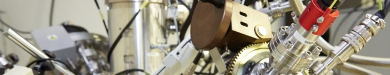
Focused Ion Beam/Scanning Electron Microscope TESCAN LYRA3 (LYRA)

Guarantor:
Tomáš Šamořil, Ph.D.
Instrument status:
![]() Operational, 17.4.2024 11:09
Operational, 17.4.2024 11:09
Equipment placement:
CEITEC Nano - C1.24
Facility for novel methods for lithographic fabrication and manipulation of nanostructures combining Scanning Electron Microscope and Focused Ion Beam Source (i.e. “Dual Beam”) equipped with 4 nanomanipulators (and photon detectors); Scanning Probe Microscopy for Fabrication of Nanostructures by local anodic oxidation and other methods.
Publications:
-
Thalluri, S. M.; Rodriguez‐Pereira, J.; Michalicka, J.; Kolíbalová, E.; Hromadko, L.; Slang, S.; Pouzar, M.; Sopha, H.; Zazpe, R.; Macak, J. M., 2025: Enhancing Alkaline Hydrogen Evolution Reaction on Ru- Decorated TiO2 Nanotube Layers: Synergistic Role of Ti3+, Ru Single Atoms, and Ru Nanoparticles. ENERGY & ENVIRONMENTAL MATERIALS , doi: 10.1002/eem2.12864; FULL TEXT
(TITAN, LYRA, KRATOS-XPS, RIGAKU3, ALD) -
OLIVER URRUTIA, C.; KASHIMBETOVA, A.; SLÁMEČKA, K.; CASAS LUNA, M.; MATULA, J.; KOLEDOVÁ, Z.; KAISER, J.; ČELKO, L.; MONTUFAR JIMENEZ, E., 2025: Porous titanium/hydroxyapatite interpenetrating phase composites with optimal mechanical and biological properties for personalized bone repair. BIOMATERIALS ADVANCES 166, p. 1 - 11, doi: 10.1016/j.bioadv.2024.214079; FULL TEXT
(micro-CT-L240, RIGAKU3, LYRA) -
HAVLÍKOVÁ, T.; PAPEŽ, N.; FOHLEROVÁ, Z.; KASPAR, P.; DALLAEV, R.; ČÁSTKOVÁ, K.; ŢĂLU, Ş., 2025: Adaptability of Electrospun PVDF Nanofibers in Bone Tissue Engineering. POLYMERS 17(3), doi: 10.3390/polym17030330; FULL TEXT
(DIENER, LYRA, WITEC-RAMAN, FTIR, SEE-SYSTEM) -
Pham, N. S.; Hong, N. H., 2025: Modulation of room temperature ferromagnetism in WO3 thin films on low-cost Si wafers. SOLID STATE COMMUNICATIONS 397, doi: 10.1016/j.ssc.2024.115807; FULL TEXT
(LYRA, KRATOS-XPS, VERSALAB, RIGAKU3, ICON-SPM, WOOLLAM-VIS, ) -
Nandi, S.; Sonigara, K. K.; Pumera, M., 2025: Exploring the electrochemistry of Al3+ ion in amorphous Bi4V2O11 for rechargeable aqueous aluminum-ion battery. APPLIED MATERIALS TODAY 42, p. 1 - 9, doi: 10.1016/j.apmt.2024.102568; FULL TEXT
(RIGAKU3, LYRA, KRATOS-XPS, BET-DEGASSER, BET-ANAMET)
-
KEPIČ, P.; LIŠKA, P.; IDESOVÁ, B.; CAHA, O.; LIGMAJER, F.; ŠIKOLA, T., 2024: Pulsed laser deposition of Sb2S3 films for phase-change tunable nanophotonics. NEW JOURNAL OF PHYSICS 26(1), p. 1 - 8, doi: 10.1088/1367-2630/ad1696; FULL TEXT
(ICON-SPM, KRATOS-XPS, LYRA, ALD, WITEC-RAMAN, RIGAKU9, WOOLLAM-VIS) -
NOUSEEN, S.; GHOSH, K.; PUMERA, M., 2024: Hydrofluoric acid-free etched MAX on 3D-printed nanocarbon electrode for photoelectrochemical hydrogen production. APPLIED MATERIALS TODAY 36, doi: 10.1016/j.apmt.2023.101995; FULL TEXT
(RIGAKU3, VERIOS, LYRA, KRATOS-XPS, JASCO) -
Mouralova, K.; Zahradnicek, R.; Benes, L.; Fries, J., 2024: Analysis of spherical chips after grinding. MEASUREMENT 229, doi: 10.1016/j.measurement.2024.114401; FULL TEXT
(LYRA) -
NOUSEEN, S.; GHOSH, K.; PUMERA, M., 2024: 3D printing of MAX/PLA filament: Electrochemical in-situ etching for enhanced energy conversion and storage. ELECTROCHEMISTRY COMMUNICATIONS 160, doi: 10.1016/j.elecom.2023.107652; FULL TEXT
(VERIOS, LYRA, KRATOS-XPS, RIGAKU3) -
KLÍMA, J.; WOJEWODA, O.; ROUČKA, V.; MOLNÁR, T.; HOLOBRÁDEK, J.; URBÁNEK, M., 2024: Zero-field spin wave turns. APPLIED PHYSICS LETTERS 124(11), doi: 10.1063/5.0189394; FULL TEXT
(BRILLOUIN, EVAPORATOR, LYRA, KERR-MICROSCOPE, RAITH, ICON-SPM) -
Mouralova, K.; Benes, L.; Fries, J., 2024: Comparison of MRR of different WEDM-machined materials. THE INTERNATIONAL JOURNAL OF ADVANCED MANUFACTURING TECHNOLOGY 132(9-10), p. 4461 - 4471, doi: 10.1007/s00170-024-13631-7; FULL TEXT
(TEGRAMIN, LYRA, DEKTAK) -
Sitek, T., 2024: Thermal decomposition of solid biofuels and associated fine particle generation. PH.D. THESIS ; FULL TEXT
(LYRA, LEICACOAT-STAN) -
Izák, J.; Benč, M.; Kunčická, L.; Opěla, P.; Kocich, R., 2024: Influence of Imposed Strain on Weldability of Dievar Alloy. MATERIALS 17(10), doi: 10.3390/ma17102317; FULL TEXT
(LYRA) -
DRDLÍKOVÁ, K.; KLEMENT, R.; RYCHNOVSKÝ, D.; MACA, K.; DRDLÍK, D., 2024: Optical properties of Tb3+- and Cr3+-doped MgAl2O4 ceramics prepared by capsule- and carbon-free hot isostatic pressing. JOURNAL OF THE EUROPEAN CERAMIC SOCIETY 44(9), p. 5440 - 9, doi: 10.1016/j.jeurceramsoc.2023.11.038; FULL TEXT
(LYRA) -
NOUSEEN, S.; DESHMUKH, S.; PUMERA, M., 2024: Nanoarchitectonics of Laser Induced MAX 3D-Printed Electrode for Photo-Electrocatalysis and Energy Storage Application with Long Cyclic Durability of 100 000 Cycles. ADVANCED FUNCTIONAL MATERIALS 34(45), p. 1 - 12, doi: 10.1002/adfm.202407071; FULL TEXT
(VERIOS, LYRA, RIGAKU3, KRATOS-XPS, WITEC-RAMAN, JASCO) -
ŠVÁBENSKÁ, E.; ROUPCOVÁ, P.; HAVLÍČEK, L.; SCHNEEWEISS, O., 2024: PROPERTIES OF NANOCRYSTALLINE Fe-Ni PARTICLES PREPARED BY THERMAL REDUCTION OF OXALATE PRECURSORS. PROCEEDINGS 12TH INTERNATIONAL CONFERENCE ON NANOMATERIALS - RESEARCH & APPLICATION , p. 76 - 6, doi: 10.37904/nanocon.2023.4773; FULL TEXT
(LYRA) -
Changela, HG.; Kebukawa, Y.; Petera, L.; Ferus, M.; Chatzitheodoridis, E.; Nejdl, L.; Nebel, R.; Protiva, V.; Krepelka, P.; Moravcova, J.; Holbova, R.; Hlavenkova, Z.; Samoril, T.; Bridges, JC.; Yamashita, S.; Takahashi, Y.; Yada, T.; Nakato, A.; Sobotkova, K.; Tesarova, H. ; Zapotok, D., 2024: The evolution of organic material on Asteroid 162173 Ryugu and its delivery to Earth. NATURE COMMUNICATIONS 15(1), doi: 10.1038/s41467-024-50004-w; FULL TEXT
(LYRA) -
TKACHENKO, S.; OLIVER URRUTIA, C.; KSENZOVA, O.; SLÁMEČKA, K.; BEDNAŘÍKOVÁ, V.; REMEŠOVÁ, M.; BALÁŽ, M.; DEÁK, A.; MONTUFAR JIMENEZ, E.; ČELKO, L., 2024: Production of spherical Mo and Mo-Si powders by spray drying of Si suspension in a water-soluble Mo precursor. ADVANCED POWDER TECHNOLOGY 35(1), doi: 10.1016/j.apt.2023.104313; FULL TEXT
(RIGAKU3, LYRA, LEICACOAT-STAN) -
KRPENSKÝ, J.; HORÁK, M.; KABÁT, J.; PLANER, J.; KEPIČ, P.; KŘÁPEK, V.; KONEČNÁ, A., 2024: Analytical electron microscopy analysis of insulating and metallic phases in nanostructured vanadium dioxide. NANOSCALE ADVANCES 6(13), p. 3338 - 9, doi: 10.1039/d4na00338a; FULL TEXT
(TITAN, LYRA, EVAPORATOR) -
Šimek, A.; Kazda, T.; Šedina, M.; Čech, O., 2024: Utilization of anthracite as electroactive material in sodium-ion batteries. MONATSHEFTE FÜR CHEMIE - CHEMICAL MONTHLY 155(3-4), p. 261 - 266, doi: 10.1007/s00706-023-03157-1; FULL TEXT
(KRATOS-XPS, LYRA) -
Švábenská, E.; Roupcová, P.; Havlíček, L.; Schneeweiss, O., 2024: Mössbauer and magnetic studies on nanocrystalline FeNi particles prepared by thermal reduction. JOURNAL OF RADIOANALYTICAL AND NUCLEAR CHEMISTRY , doi: 10.1007/s10967-024-09898-5; FULL TEXT
(LYRA, RIGAKU3) -
MAŘÁK, V.; DRDLÍK, D.; BIJALWAN, V.; TOFEL, P.; ERHART, J.; CHLUP, Z.; MACA, K., 2024: Effect of alumina or zirconia particles on the performance of lead-free BCZT piezoceramics. CERAMICS INTERNATIONAL 50(24), p. 53491 - 11, doi: 10.1016/j.ceramint.2024.10.199; FULL TEXT
(LYRA, RIGAKU3) -
KOVAŘÍK, M.; CITTERBERG, D.; PAIVA DE ARAÚJO, E.; ŠIKOLA, T.; KOLÍBAL, M., 2024: Understanding the Effect of Electron Irradiation on WS2 Nanotube Devices to Improve Prototyping Routines. ACS APPLIED ELECTRONIC MATERIALS 6(12), p. 8776 - 7, doi: 10.1021/acsaelm.4c01450; FULL TEXT
(ALD, MIRA-EBL, EVAPORATOR, MPS150, KEITHLEY-4200, LYRA, LITESCOPE-LYRA, WITEC-RAMAN, WIRE-BONDER) -
KANDAMBATH PADINJAREVEETIL, A.; PUMERA, M., 2024: Downsizing nanoarchitectonics of multilayered MXenes electrocatalysts towards real time ion tracking via EQCM and electrocatalytic applications. CARBON 226, doi: 10.1016/j.carbon.2024.119228; FULL TEXT
(LYRA, KRATOS-XPS, RIGAKU3) -
Mouralova, K.; Fries, J.; Benes, L.; Houska, P., 2024: Materials That Do Not Form Any Defects After WEDM. PROCESSES 12(11), doi: 10.3390/pr12112448; FULL TEXT
(DEKTAK, LYRA, TEGRAMIN) -
Mouralova, K.; Bednar, J.; Benes, L.; Prokes, T.; Zahradnicek, R.; Fries, J., 2023: Mathematical Models for Machining Optimization of Ampcoloy 35 with Different Thicknesses Using WEDM to Improve the Surface Properties of Mold Parts. MATERIALS 16(1), doi: 10.3390/ma16010100; FULL TEXT
(TEGRAMIN, DEKTAK, LYRA) -
Benes, L.; Mouralova, K.; Midula, P.; Snow, J.; Lysonkova, I.; Pilnaj, D.; Burdova, H.; Prokes, T.; Zahradnicek, R.; Fries, J.; Kuráň, P.; Kubenka, M., 2023: The Corrosion Behavior of WEDM Machined Stainless Steels in a Pyrolysis Environment. METALS 13(1), doi: 10.3390/met13010144; FULL TEXT
(DEKTAK, TEGRAMIN, LYRA) -
PALACIOS CORELLA, M.; ROJAS TIZÓN, J.; PUMERA, M., 2023: Photocatalytic Pt/Ag3VO4 micromotors with inherent sensing capabilities for corroding environments. JOURNAL OF COLLOID AND INTERFACE SCIENCE 631, p. 125 - 10, doi: 10.1016/j.jcis.2022.10.169; FULL TEXT
(KRATOS-XPS, FTIR, RIGAKU3, LYRA) -
Mouralova, K.; Benes, L.; Prokes, T.; Zahradnicek, R.; Fries, J.; Plichta, T., 2023: Analysis of the machinability of different types of sintered carbides with WEDM in both water and oil baths. INTERNATIONAL JOURNAL OF ADVANCED MANUFACTURING TECHNOLOGY 125(5-6), p. 2705 - 2715, doi: 10.1007/s00170-023-10913-4; FULL TEXT
(DEKTAK, LYRA) -
Hu, S.; Wang, D.; Křemenáková, D.; Militký, J., 2023: Washable and breathable ultrathin copper-coated nonwoven polyethylene terephthalate (PET) fabric with chlorinated poly-para-xylylene (parylene-C) encapsulation for electromagnetic interference shielding application. TEXTILE RESEARCH JOURNAL , doi: 10.1177/00405175231168418; FULL TEXT
(PARYLENE-SCS, LYRA) -
GABLECH, I.; MIGLIACCIO, L.; BRODSKÝ, J.; HAVLÍČEK, M.; PODEŠVA, P.; HRDÝ, R.; EHLICH, J.; GRYSZEL, M.; GLOWACKI, E., 2023: High-Conductivity Stoichiometric Titanium Nitride for Bioelectronics. ADVANCED ELECTRONIC MATERIALS 9(4), p. 1 - 11, doi: 10.1002/aelm.202200980; FULL TEXT
(KAUFMAN, PARYLENE-SCS, KRATOS-XPS, RIGAKU3, KEITHLEY-4200, LYRA, ICON-SPM) -
SEPÚLVEDA SEPÚLVEDA, L.; SALDAN, I.; ALIJANI, M.; ČIČMANCOVÁ, V.; MICHALIČKA, J.; HROMÁDKO, L.; BULÁNEK, R.; SOPHA, H.; MACÁK, J., 2023: Magnetically guidable single TiO2 nanotube photocatalyst: Structure and photocatalytic properties. CERAMICS INTERNATIONAL 49(4), p. 6764 - 8, doi: 10.1016/j.ceramint.2022.10.197; FULL TEXT
(TITAN, LYRA) -
WOJEWODA, O.; LIGMAJER, F.; HRTOŇ, M.; KLÍMA, J.; DHANKHAR, M.; DAVÍDKOVÁ, K.; STAŇO, M.; HOLOBRÁDEK, J.; KRČMA, J.; ZLÁMAL, J.; ŠIKOLA, T.; URBÁNEK, M., 2023: Observing high-k magnons with Mie-resonance-enhanced Brillouin light scattering. COMMUNICATIONS PHYSICS 6(1), p. 1 - 10, doi: 10.1038/s42005-023-01214-z; FULL TEXT
(RAITH, MIRA-EBL, EVAPORATOR, MAGNETRON, ALD, LYRA, ICON-SPM, BRILLOUIN) -
MUNOZ MARTIN, J.; OLIVER DE LA CRUZ, J.; FORTE, G.; PUMERA, M., 2023: Graphene-based 3D-Printed nanocomposite bioelectronics for monitoring breast cancer cell adhesion. BIOSENSORS & BIOELECTRONICS 226, doi: 10.1016/j.bios.2023.115113; FULL TEXT
(KRATOS-XPS, LYRA) -
Šmíd, M.; Koutný, D.; Neumannová, K.; Chlup, Z.; Náhlík, L.; Jambor, M., 2023: Cyclic behaviour and microstructural evolution of metastable austenitic stainless steel 304L produced by laser powder bed fusion. ADDITIVE MANUFACTURING 68, doi: 10.1016/j.addma.2023.103503; FULL TEXT
(LYRA, TITAN, LECTROPOL) -
JANŮ, L.; DVOŘÁKOVÁ, E.; POLÁŠKOVÁ, K.; BUCHTELOVÁ, M.; RYŠÁNEK, P.; CHLUP, Z.; KRUML, T.; GALMIZ, O.; NEČAS, D.; ZAJÍČKOVÁ, L., 2023: Enhanced Adhesion of Electrospun Polycaprolactone Nanofibers to Plasma-Modified Polypropylene Fabric. POLYMERS 15(7), p. 1 - 17, doi: 10.3390/polym15071686; FULL TEXT
(LYRA, LEICACOAT-STAN, KRATOS-XPS, SEE-SYSTEM) -
WOJEWODA, O.; HRTOŇ, M.; DHANKHAR, M.; KRČMA, J.; DAVÍDKOVÁ, K.; KLÍMA, J.; HOLOBRÁDEK, J.; LIGMAJER, F.; ŠIKOLA, T.; URBÁNEK, M., 2023: Phase-resolved optical characterization of nanoscale spin waves. APPLIED PHYSICS LETTERS 122(20), p. 1 - 6, doi: 10.1063/5.0151338; FULL TEXT
(RAITH, BRILLOUIN, LYRA, MAGNETRON, EVAPORATOR) -
POLAT, Ö.; HORÁK, M.; ARREGI URIBEETXEBARRIA, J.; BUKVIŠOVÁ, K.; ZLÁMAL, J.; ŠIKOLA, T., 2023: Synthesis and characterization of half-Heusler ScPtBi films via three-source magnetron co-sputtering on Nb superconductor buffer layer. SURFACES AND INTERFACES 40, doi: 10.1016/j.surfin.2023.103118; FULL TEXT
(MAGNETRON, RIGAKU9, TITAN, HELIOS, KRATOS-XPS, CRYOGENIC, LYRA) -
Bevz, VM.; Mikhailov, MY.; Budinska, B.; Lamb-Camarena, S.; Shpilinska, SO.; Chumak, AV.; Urbanek, M.; Arndt, M.; Lang, W.; Dobrovolskiy, OV., 2023: Vortex Counting and Velocimetry for Slitted Superconducting Thin Strips. PHYSICAL REVIEW APPLIED 19(3), doi: 10.1103/PhysRevApplied.19.034098; FULL TEXT
(DWL, LYRA, EVAPORATOR) -
Klíma, J., 2023: Spin waves in non-trivial magnetic landscapes. BACHELOR´S THESIS , p. 1 - 69; FULL TEXT
(MIRA-EBL, LYRA, ICON-SPM, KERR-MICROSCOPE, BRILLOUIN, EVAPORATOR) -
LIŠKA, P.; MUSÁLEK, T.; ŠAMOŘIL, T.; KRATOCHVÍL, M.; MATULA, R.; HORÁK, M.; NEDVĚD, M.; URBAN, J.; PLANER, J.; ROVENSKÁ, K.; DVOŘÁK, P.; KOLÍBAL, M.; KŘÁPEK, V.; KALOUSEK, R.; ŠIKOLA, T., 2023: Correlative Imaging of Individual CsPbBr3 Nanocrystals: Role of Isolated Grains in Photoluminescence of Perovskite Polycrystalline Thin Films. JOURNAL OF PHYSICAL CHEMISTRY C (PRINT) 127(25), p. 12404 - 10, doi: 10.1021/acs.jpcc.3c03056; FULL TEXT
(LYRA, VERIOS, ICON-SPM, WITEC-RAMAN, KRATOS-XPS, TITAN) -
Mouralova, K.; Bednar, J.; Benes, L.; Polzer, A.; Zahradnicek, R.; Fries, J.; Prokes, T., 2023: Machining of 1.2363 and 1.2343ESR steels using EDM. JOURNAL OF THE BRAZILIAN SOCIETY OF MECHANICAL SCIENCES AND ENGINEERING 45(7), doi: 10.1007/s40430-023-04293-9; FULL TEXT
(DEKTAK, LYRA, TITAN, HELIOS, TEGRAMIN) -
Kuběna, I.; Fintová, S.; Jambor, M.; Šmíd, M., 2023: TKD/EBSD and TEM analysis of microstructural changes ongoing in AISI 304L steel exposed to the cyclic loading. MATERIALS SCIENCE AND ENGINEERING: A 872, doi: 10.1016/j.msea.2023.144943; FULL TEXT
(TITAN, LYRA) -
TKACHENKO, S.; BEDNAŘÍKOVÁ, V.; KSENZOVA, O.; REMEŠOVÁ, M.; SLÁMEČKA, K.; CIHLÁŘ, J.; BALÁŽ, M.; DEÁK, A.; ČELKO, L., 2023: Microstructure and reduction behavior of Mo powders doped with La2O3 and ZrO2 oxides using the spray drying method. JOURNAL OF ALLOYS AND COMPOUNDS 264, doi: 10.1016/j.jallcom.2023.171307; FULL TEXT
(RIGAKU3, LYRA, KRATOS-XPS, LEICACOAT-NANO) -
JYOTI, J.; FOJTA, M.; HERMANOVÁ, M.; PIVOŇKOVÁ, H.; ALDUHAISH, O.; PUMERA, M., 2023: Genosensing on a 3D-printed nanocarbon electrode. ELECTROCHEMISTRY COMMUNICATIONS 151, doi: 10.1016/j.elecom.2023.107508; FULL TEXT
(LYRA, KRATOS-XPS) -
GAO, W.; PERALES RONDON, J.; MICHALIČKA, J.; PUMERA, M., 2023: Ultrathin manganese oxides enhance the electrocatalytic properties of 3D printed carbon catalysts for electrochemical nitrate reduction to ammonia. APPLIED CATALYSIS B: ENVIRONMENTAL 330, doi: 10.1016/j.apcatb.2023.122632; FULL TEXT
(ALD, VERIOS, LYRA, TITAN, KRATOS-XPS, JASCO) -
PAREDES SÁNCHEZ, C.; ROLEČEK, J.; PEJCHALOVÁ, L.; SPUSTA, T.; SALAMON, D.; MIRANDA, P., 2023: Evaluating the suitability of fast sintering techniques for the consolidation of calcium phosphate scaffolds produced by DLP. JOURNAL OF THE EUROPEAN CERAMIC SOCIETY 43(14), p. 6493 - 11, doi: 10.1016/j.jeurceramsoc.2023.05.052; FULL TEXT
(VERIOS, LYRA, RIGAKU3) -
KANDAMBATH PADINJAREVEETIL, A.; PERALES RONDON, J.; ZAORALOVÁ, D.; OTYEPKA, M.; ALDUHAISH, O.; PUMERA, M., 2023: Fe-MOF Catalytic Nanoarchitectonic toward Electrochemical Ammonia Production. ACS APPLIED MATERIALS & INTERFACES 15(40), p. 47294 - 13, doi: 10.1021/acsami.3c12822; FULL TEXT
(LYRA, VERIOS, JASCO, KRATOS-XPS, RIGAKU3) -
SALAMON, D.; BUKVIŠOVÁ, K.; JAN, V.; POTOČEK, M.; ČECHAL, J., 2023: Superflux of an organic adlayer towards its local reactive immobilization. COMMUNICATIONS CHEMISTRY 6(1), doi: 10.1038/s42004-023-01020-2; FULL TEXT
(KRATOS-XPS, SIMS, LYRA, LITESCOPE-LYRA) -
PALACIOS CORELLA, M.; SANNA, M.; MUNOZ MARTIN, J.; GHOSH, K.; WERT, S.; PUMERA, M., 2023: Heterolayered carbon allotrope architectonics via multi-material 3D printing for advanced electrochemical devices. VIRTUAL AND PHYSICAL PROTOTYPING 18(1), doi: 10.1080/17452759.2023.2276260; FULL TEXT
(LYRA, KRATOS-XPS, WITEC-RAMAN, RIGAKU3) -
DRDLÍK, D.; DRDLÍKOVÁ, K.; MACA, K., 2023: Dilatometric and microstructural study of particle and functionally graded composites based on hydroxyapatite and crystalline bioglass. SCIENCE OF SINTERING 55, p. 289 - 18, doi: 10.2298/SOS221028017D; FULL TEXT
(RIGAKU3, LYRA) -
JYOTI, J.; MUNOZ MARTIN, J.; PUMERA, M., 2023: Quantum Material-Based Self-Propelled Microrobots for the Optical ´On-the-Fly´ Monitoring of DNA. ACS APPLIED MATERIALS & INTERFACES 15(50), p. 58548 - 8, doi: 10.1021/acsami.3c09920; FULL TEXT
(LYRA, JASCO, FTIR-CHEMLAB) -
PONGRÁCZ, J.; VACEK, P.; GRÖGER, R., 2023: Recombination activity of threading dislocations in MOVPE-grown AlN/Si {111} films etched by phosphoric acid. JOURNAL OF APPLIED PHYSICS 134(19), doi: 10.1063/5.0171937; FULL TEXT
(LYRA, ICON-SPM, HELIOS, TITAN, LEICACOAT-NANO) -
Paredes, C.; Roleček, J.; Pejchalová, L.; Spusta, T.; Salamon, D.; Miranda, P., 2023: Evaluating the suitability of fast sintering techniques for the consolidation of calcium phosphate scaffolds produced by DLP. JOURNAL OF THE EUROPEAN CERAMIC SOCIETY 43(14), p. 6493 - 6503, doi: 0.1016/j.jeurceramsoc.2023.05.052; FULL TEXT
(VERIOS, LYRA, RIGAKU3) -
Švábenská, E.; Roupcová, P.; Friák, M.; Schneeweiss, O., 2023: Nanoparticles from brake pads wear. NANOCON CONFERENCE PROCEEDINGS 2022 , p. 249 - 254, doi: 10.37904/nanocon.2022.4616; FULL TEXT
(RIGAKU3, LYRA) -
POLAT, Ö.; ARREGI URIBEETXEBARRIA, J.; HORÁK, M.; POLČÁK, J.; BUKVIŠOVÁ, K.; ZLÁMAL, J.; ŠIKOLA, T., 2022: The fabrication and characterization of half-Heusler YPdBi thin films. JOURNAL OF PHYSICS AND CHEMISTRY OF SOLIDS 161, p. 1 - 6, doi: 10.1016/j.jpcs.2021.110447; FULL TEXT
(MAGNETRON, RIGAKU9, TITAN, HELIOS, KRATOS-XPS, CRYOGENIC, LYRA) -
ČELKO, L.; TKACHENKO, S.; CASAS LUNA, M.; DYČKOVÁ, L.; BEDNAŘÍKOVÁ, V.; REMEŠOVÁ, M.; KOMAROV, P.; DEÁK, A.; BALÁŽ, M.; CRAWFORD, D.; DÍAZ DE LA TORRE, S.; BODOKI, E.; CIHLÁŘ, J., 2022: High-energy ball milling and spark plasma sintering of molybdenum - lanthanum oxide (Mo-La2O3) and molybdenum - lanthanum zirconate (Mo-La2Zr2O7) composite powders. INTERNATIONAL JOURNAL OF REFRACTORY METALS & HARD MATERIALS 102, p. 1 - 13, doi: 10.1016/j.ijrmhm.2021.105717; FULL TEXT
(RIGAKU3, LEICACOAT-STAN, LYRA) -
MENDOSA-SANDOVAL, E.; RODRIGUEZ-LOPEZ, G.; ORDONEZ-ROMERO, C.; LAY, D.; QURESHI, N.; URBÁNEK, M.; SOLIS-IBARRA, D.; NOGUEZ, C.; LARA-GARCIA, H.; PIRRUCCIO, G., 2022: Shaping and enhancing the photoluminescence of halide perovskite quantum dots with plasmonic lattices. JOURNAL OF MATERIALS CHEMISTRY C , p. 3704 - 9, doi: 10.1039/d1tc05331k; FULL TEXT
(RAITH, MAGNETRON, RIE-CHLORINE, LYRA) -
Polzer, A.; Mouralova, K.; Benes, L.; Zahradnicek, R.; Fries, J., 2022: Comparison of machinability of nickel alloys using WEDM. PROCEEDINGS OF THE INSTITUTION OF MECHANICAL ENGINEERS, PART B: JOURNAL OF ENGINEERING MANUFACTURE , doi: 10.1177/09544054221075876; FULL TEXT
(TEGRAMIN, DEKTAK, HELIOS, TITAN, LYRA) -
Midlik, Š.; Sadílek, J.; Xie, Z.; Huang, Y.; Schmoranzer, D., 2022: Silicon Vibrating Micro-Wire Resonators for Study of Quantum Turbulence in Superfluid He-4. JOURNAL OF LOW TEMPERATURE PHYSICS , doi: 10.1007/s10909-022-02675-2; FULL TEXT
(PECVD, RIE-FLUORINE, SUSS-MA8, SUSS-RCD8, EVAPORATOR, DWL, LYRA) -
PISARENKO, T.; PAPEŽ, N.; SOBOLA, D.; ŢĂLU, Ş.; ČÁSTKOVÁ, K.; ŠKARVADA, P.; MACKŮ, R.; ŠČASNOVIČ, E.; KAŠTYL, J., 2022: Comprehensive characterization of PVDF nanofibers at macro- and nanolevel. POLYMERS 14(3), p. 593 - 18, doi: 10.3390/polym14030593; FULL TEXT
(HELIOS, WITEC-RAMAN, FTIR-CHEMLAB, KRATOS-XPS, SEE-SYSTEM, LYRA) -
KASHIMBETOVA, A.; SLÁMEČKA, K.; CASAS LUNA, M.; OLIVER-URRUTIA, C.; RAVASZOVÁ, S.; DVOŘÁK, K.; ČELKO, L.; MONTUFAR JIMENEZ, E., 2022: Implications of unconventional setting conditions on the mechanical strength of synthetic bone grafts produced with self-hardening calcium phosphate pastes. CERAMICS INTERNATIONAL 48(5), p. 6225 - 11, doi: 10.1016/j.ceramint.2021.11.163; FULL TEXT
(RIGAKU3, LYRA) -
Mouralova, K.; Bednar, J.; Benes, L.; Plichta, T.; Prokes, T.; Fries, J., 2022: Production of precision slots in copper foil using micro EDM. SCIENTIFIC REPORTS 12(1), doi: 10.1038/s41598-022-08957-9; FULL TEXT
(LYRA) -
POLAT, Ö.; MOHELSKÝ, I.; ARREGI URIBEETXEBARRIA, J.; HORÁK, M.; POLČÁK, J.; BUKVIŠOVÁ, K.; ZLÁMAL, J.; ŠIKOLA, T., 2022: An investigation of structural and magnetotransport features of half-Heusler ScPtBi thin films. MATERIALS RESEARCH BULLETIN 149, p. 111696-1 - 7, doi: 10.1016/j.materresbull.2021.111696; FULL TEXT
(MAGNETRON, RIGAKU9, TITAN, HELIOS, KRATOS-XPS, CRYOGENIC, LYRA) -
DRDLÍKOVÁ, K.; KLEMENT, R.; SVOBODA, J.; DRDLÍK, D.; GALUSEK, D.; MACA, K., 2022: Luminescent Dy3+ and Dy3+/Cr3+ doped transparent Al2O3 ceramics: Microstructure and optical properties. JOURNAL OF THE EUROPEAN CERAMIC SOCIETY 42(10), p. 4343 - 10, doi: 10.1016/j.jeurceramsoc.2022.03.047; FULL TEXT
(VERIOS, TITAN, LYRA) -
Krpenský, J., 2022: Fabrication, optimization and in-situ characterization of thermally tunable vanadium dioxide nanostructures. MASTER´S THESIS ; FULL TEXT
(EVAPORATOR, UHV-PREPARATION, VERIOS, TITAN, LYRA) -
Havlínová, D., 2022: Use of unconventional technologies in the production of a selected component. MASTER´S THESIS ; FULL TEXT
(LYRA) -
Hadraba, H.; Chlup, Z.; Cizek, J.; Kubena, I., 2022: 9Cr–1W steel strengthened by AlN and BN dispersion. JOURNAL OF MATERIALS SCIENCE 57(26), p. 12572 - 12584, doi: 10.1007/s10853-022-07395-2; FULL TEXT
(TITAN, LYRA) -
BEDNAŘÍKOVÁ, V.; KLAKURKOVÁ, L.; REMEŠOVÁ, M.; HORYNOVÁ, M.; SUCHÝ, J.; PALOUŠEK, D.; ČELKO, L., 2022: In Vitro Corrosion Study of Selected Laser Melted WE43 Magnesium Alloy in Hank´s Balanced Salt Solution. KEY ENGINEERING MATERIALS (WEB) 923, p. 113 - 6, doi: 10.4028/p-i214k4
(RIGAKU3, LYRA) -
KASHIMBETOVA, A.; TKACHENKO, S.; REMEŠOVÁ, M.; MATA-LEIJA, A.; GEJDOŠ, P.; ČELKO, L.; MONTUFAR JIMENEZ, E., 2022: Correlating the Microstructure with the Mechanical Behaviour of Titanium Structures Produced by Robotic Assisted Deposition. SOLID STATE PHENOMENA 334, p. 26 - 5, doi: 10.4028/p-7v18ei; FULL TEXT
(LYRA) -
TKACHENKO, S.; ČELKO, L.; REMEŠOVÁ, M.; BEDNAŘÍKOVÁ, V.; DVOŘÁK, K.; KOMAROV, P.; ZÁBRANSKÝ, K., 2022: Microstructure of Mo-La2O3 Composite Powder Prepared Using Two Different High Energy Ball Milling Systems. SOLID STATE PHENOMENA 334, p. 109 - 6, doi: 10.4028/p-a18wu2; FULL TEXT
(LEICACOAT-STAN, RIGAKU3, LYRA) -
DRDLÍK, D.; MAŘÁK, V.; MACA, K.; DRDLÍKOVÁ, K., 2022: Modification of barium titanate sintering via rare earth oxides addition: Dilatometric and microstructural study. CERAMICS INTERNATIONAL 48(17), p. 24599 - 10, doi: 10.1016/j.ceramint.2022.05.105; FULL TEXT
(RIGAKU3, WITEC-RAMAN, LYRA) -
SVOBODA, J.; DRDLÍKOVÁ, K.; DRDLÍK, D.; KROUPA, A.; MICHALIČKA, J.; MACA, K., 2022: Doping of alumina ceramics by manganese – Thermodynamical and experimental approach. PROCESSING AND APPLICATION OF CERAMICS 16(1), p. 13 - 9, doi: 10.2298/PAC2201013S; FULL TEXT
(TITAN, LYRA) -
MANIŠ, J.; MACH, J.; BARTOŠÍK, M.; ŠAMOŘIL, T.; HORÁK, M.; ČALKOVSKÝ, V.; NEZVAL, D.; KACHTÍK, L.; KONEČNÝ, M.; ŠIKOLA, T., 2022: Low temperature 2D GaN growth on Si(111) 7 x 7 assisted by hyperthermal nitrogen ions. NANOSCALE ADVANCES 4(17), p. 1 - 8, doi: 10.1039/d2na00175f; FULL TEXT
(VERIOS, NANOSAM, TITAN, LYRA, ICON-SPM) -
MUNOZ MARTIN, J.; PALACIOS CORELLA, M.; PUMERA, M., 2022: Electrically reading a light-driven molecular switch on 2D-Ti3C2Tx MXene via molecular engineering: towards responsive MXetronics. JOURNAL OF MATERIALS CHEMISTRY A 10(32), p. 17001 - 8, doi: 10.1039/d2ta03349f; FULL TEXT
(KRATOS-XPS, FTIR, LYRA) -
DVOŘÁK, P.; KLOK, P.; KVAPIL, M.; HRTOŇ, M.; BOUCHAL, P.; KRPENSKÝ, J.; KŘÁPEK, V.; ŠIKOLA, T., 2022: Two-dimensional quantitative near-field phase imaging using square and hexagonal interference devices. NANOPHOTONICS 11(19), p. 1 - 12, doi: 10.1515/nanoph-2022-0215; FULL TEXT
(SNOM-NANONICS, LYRA) -
KANDAMBATH PADINJAREVEETIL, A.; ALDUHAISH, O.; ADIL, S.; PUMERA, M., 2022: Grafting of Pd on Covalently and Noncovalently Modified N-Doped Graphene for Electrocatalysis. ADVANCED MATERIALS INTERFACES 9(27), p. 2102317 - 8, doi: 10.1002/admi.202102317; FULL TEXT
(MIRA-STAN, KRATOS-XPS, LYRA) -
KADIEV, M.; SHUAIBOV, A.; ABDURAKHMANOV, M.; SELIMOV, D.; GULAKHMEDOV, R.; RABADANOVA, A.; SMEJKALOVÁ, T.; SOBOLA, D.; ČÁSTKOVÁ, K.; RAMAZANOV, S.; ORUDZHEV, F., 2022: Synthesis and Investigation of Piezophotocatalytic Properties of Polyvinylidene Fluoride Nanofibers Modified with Titanium Dioxide. MOSCOW UNIVERSITY CHEMISTRY BULLETIN , p. 256 - 6, doi: 10.3103/S0027131422050054; FULL TEXT
(LEICACOAT-NANO, LYRA) -
MUNOZ MARTIN, J.; PALACIOS CORELLA, M.; GOMEZ PEREZ, I.; ZAJÍČKOVÁ, L.; PUMERA, M., 2022: Synthetic Nanoarchitectonics of Functional Organic-Inorganic 2D Germanane Heterostructures via Click Chemistry. ADVANCED MATERIALS 45(34), doi: 10.1002/adma.202206382; FULL TEXT
(KRATOS-XPS, RIGAKU3, FTIR, WITEC-RAMAN, LYRA, ICON-SPM) -
Mouralova, K.; Benes, L.; Prokes, T.; Bednar, J.; Zahradnicek, R.; Fries, J., 2022: Analysis of the effect of material thickness during the WEDM processon cutting speed, topography and morphology. PROCEEDINGS OF THE INSTITUTION OF MECHANICAL ENGINEERS, PART B: JOURNAL OF ENGINEERING MANUFACTURE , doi: 10.1177/09544054221136516; FULL TEXT
(TEGRAMIN, DEKTAK, LYRA) -
PAREDES SÁNCHEZ, C.; ROLEČEK, J.; PEJCHALOVÁ, L.; MIRANDA MENDES, J.; SALAMON, D., 2022: Impact of residual carbon after DLP and SPS-Sintering on compressive strength and in-VITRO bioactivity of calcium phosphate scaffolds. OPEN CERAMICS 11, p. 100281-1 - 9, doi: 10.1016/j.oceram.2022.100281; FULL TEXT
(RIGAKU3, VERIOS, LYRA) -
PALACIOS CORELLA, M.; MUNOZ MARTIN, J.; PUMERA, M., 2022: Molecularly ´clicking´ active moieties to germanium-based inorganic 2D materials. NANOSCALE 14(48), p. 18167 - 8, doi: 10.1039/d2nr04955d; FULL TEXT
(KRATOS-XPS, FTIR, WITEC-RAMAN, RIGAKU3, LYRA) -
CASAS LUNA, M.; MONTUFAR JIMENEZ, E.; HORT, N.; DÍAZ DE LA TORRE, S.; MENDEZ-GARCIA, J.; VIŠTEJNOVÁ, L.; BŘÍNEK, A.; DAŇHEL, A.; DVOŘÁK, K.; KAISER, J.; ČELKO, L., 2022: Degradable magnesium-hydroxyapatite interpenetrating phase composites processed by current assisted metal infiltration in additive-manufactured porous preforms. JOURNAL OF MAGNESIUM AND ALLOYS 10(12), p. 3641 - 16, doi: 10.1016/j.jma.2022.07.019; FULL TEXT
(RIGAKU3, micro-CT-L240, LYRA) -
SPUSTA, T.; PRAJZLER, V.; MACA, K., 2022: Grain growth during capsule-free hot isostatic pressing. CERAMICS INTERNATIONAL 48(18), p. 25764 - 8, doi: 10.1016/j.ceramint.2022.05.248; FULL TEXT
(LYRA) -
Fridrišek, T., 2022: Optical gating of epitaxial graphene. MASTER´S THESIS
(MIRA-EBL, RIE-FLUORINE, EVAPORATOR, WIRE-BONDER, LYRA) -
Řepa, R., 2022: Plasmonic lightning-rod effect. BACHELOR´S THESIS , p. 1 - 43; FULL TEXT
(LYRA, TITAN) -
Děcký, M., 2022: Fabrication and testing of microbolometer or other infrared detector based on plasmonic antennas. BACHELOR´S THESIS , p. 1 - 44; FULL TEXT
(LYRA, MIRA-EBL, EVAPORATOR, DWL, MPS150) -
Turčan, I., 2022: Magnetism in curved geometries. PH.D. THESIS , p. 1 - 117; FULL TEXT
(LYRA, BRILLOUIN, ICON-SPM, MIRA-EBL, KERR-MICROSCOPE, HELIOS) -
GAO, W.; PUMERA, M., 2021: 3D Printed Nanocarbon Frameworks for Li-Ion Battery Cathodes. ADVANCED FUNCTIONAL MATERIALS , p. 2007285-1 - 10, doi: 10.1002/adfm.202007285; FULL TEXT
(VERIOS, KRATOS-XPS, LYRA) -
ŠIMŮNKOVÁ, H.; LEDNICKÝ, T.; WHITEHEAD, A.; KALINA, L.; ŠIMŮNEK, P.; HUBÁLEK, J., 2021: Tantalum-based nanotube arrays via porous-alumina-assisted electrodeposition from ionic liquid: Formation and electrical characterization. APPLIED SURFACE SCIENCE 548, p. 149264 - 10, doi: 10.1016/j.apsusc.2021.149264; FULL TEXT
(LYRA, ICON-SPM) -
REDONDO NEGRETE, E.; PUMERA, M., 2021: MXene-functionalised 3D-printed electrodes for electrochemical capacitors. ELECTROCHEMISTRY COMMUNICATIONS 124, p. 1 - 6, doi: 10.1016/j.elecom.2021.106920; FULL TEXT
(KRATOS-XPS, WITEC-RAMAN, LYRA) -
Vaňatka, M., 2021: Static and dynamic properties of nanostructured magnetic materials. PH.D. THESIS , p. 1 - 113; FULL TEXT
(VERSALAB, VNA-MPI, TITAN, BRILLOUIN, MIRA-EBL, RAITH, KERR-MICROSCOPE, MAGNETRON, EVAPORATOR, VERIOS, WIRE-BONDER, LYRA) -
Muñoz, J.; Redondo, E.; Pumera, M., 2021: Bistable (Supra)molecular Switches on 3D-Printed Responsive Interfaces with Electrical Readout. ACS APPLIED MATERIALS & INTERFACES 13(11), p. 12649 - 12655, doi: 10.1021/acsami.0c14487; FULL TEXT
(KRATOS-XPS, LYRA) -
WANG, L.; GAO, W.; NG, S.; PUMERA, M., 2021: Chiral Protein-Covalent Organic Framework 3D-Printed Structures as Chiral Biosensors. ANALYTICAL CHEMISTRY 93(12), p. 5277 - 7, doi: 10.1021/acs.analchem.1c00322; FULL TEXT
(VERIOS, KRATOS-XPS, LYRA) -
MUNOZ MARTIN, J.; REDONDO NEGRETE, E.; PUMERA, M., 2021: Chiral 3D-printed Bioelectrodes. ADVANCED FUNCTIONAL MATERIALS 31(16), p. 2010608-1 - 9, doi: 10.1002/adfm.202010608; FULL TEXT
(KRATOS-XPS, WITEC-RAMAN, LYRA) -
ŠŤASTNÝ, P.; CHLUP, Z.; ČÁSTKOVÁ, K.; TRUNEC, M., 2021: High strength alumina tapes prepared by gel-tape casting method. CERAMICS INTERNATIONAL 47(5), p. 6988 - 8, doi: 10.1016/j.ceramint.2020.11.048; FULL TEXT
(VERIOS, LYRA) -
OLIVER, C.; IBANEZ, R.; FLORES-MERINO, M.; VOJTOVÁ, L.; ŠALPLACHTA, J.; ČELKO, L.; KAISER, J.; MONTUFAR JIMENEZ, E., 2021: Lyophilized Polyvinylpyrrolidone Hydrogel for Culture of Human Oral Mucosa Stem Cells. MATERIALS 14(1), p. 1 - 14, doi: 10.3390/ma14010227; FULL TEXT
(FTIR, WITEC-RAMAN, LYRA) -
NOVCIC, K.; IFFELSBERGER, C.; NG, S.; PUMERA, M., 2021: Local electrochemical activity of transition metal dichalcogenides and their heterojunctions on 3D-printed nanocarbon surfaces. NANOSCALE 13(10), p. 5324 - 9, doi: 10.1039/d0nr06679f; FULL TEXT
(KRATOS-XPS, LYRA) -
MICHLÍČEK, M.; BLAHOVÁ, L.; DVOŘÁKOVÁ, E.; NEČAS, D.; ZAJÍČKOVÁ, L., 2021: Deposition penetration depth and sticking probability in plasma polymerization of cyclopropylamine. APPLIED SURFACE SCIENCE 540, p. 1 - 10, doi: 10.1016/j.apsusc.2020.147979; FULL TEXT
(WOOLLAM-VIS, FTIR, KRATOS-XPS, LYRA) -
Zadorozhnii, O., 2021: Exchange bias in metamagnetic heterostructures. MASTER´S THESIS , p. 1 - 81; FULL TEXT
(MAGNETRON, VERSALAB, KERR-MICROSCOPE, RAITH, RIE-FLUORINE, UHV-DEPOSITION, UHV-PREPARATION, UHV-XPS, LYRA) -
Vinogradov, A.; Heczko, M.; Mazánová, V.; Linderov, M.; Kruml, T., 2021: Kinetics of cyclically-induced mechanical twinning in γ-TiAl unveiled by a combination of acoustic emission, neutron diffraction and electron microscopy. ACTA MATERIALIA 212, doi: 10.1016/j.actamat.2021.116921; FULL TEXT
(TITAN, LYRA) -
Brodský J., 2021: Gas sensors based on 1D and 2D materials. MASTER´S THESIS , p. 1 - 84; FULL TEXT
(DWL, DIENER, SUSS-RCD8, SUSS-MA8, EVAPORATOR, MPS150, WITEC-RAMAN, RIE-FLUORINE, DRIE, LYRA, ICON-SPM) -
Mouralova, K.; Polzer, A.; Benes, L.; Bednar, J.; Zahradnicek, R.; Prokes, T.; Fiala, Z.; Fries, J., 2021: Machining of B1914 nickel-based superalloy using wire electrical discharge machining. PROCEEDINGS OF THE INSTITUTION OF MECHANICAL ENGINEERS, PART E: JOURNAL OF PROCESS MECHANICAL ENGINEERING , doi: 10.1177/09544089211031746; FULL TEXT
(TEGRAMIN, DEKTAK, HELIOS, TITAN, LYRA) -
Kepič, P., 2021: Design and fabrication of tunable dielectric metasurfaces for visible and infrared wavelengths. MASTER´S THESIS , p. 1 - 76; FULL TEXT
(MIRA-EBL, EVAPORATOR, DEKTAK, WITEC-RAMAN, KRATOS-XPS, SNOM-NANONICS, LYRA, ICON-SPM) -
TURČAN, I.; FLAJŠMAN, L.; WOJEWODA, O.; ROUČKA, V.; MAN, O.; URBÁNEK, M., 2021: Spin wave propagation in corrugated waveguides. APPLIED PHYSICS LETTERS 118(9), p. 1 - 5, doi: 10.1063/5.0041138; FULL TEXT
(HELIOS, RAITH, KERR-MICROSCOPE, VERSALAB, VNA-MPI, BRILLOUIN, LYRA, ICON-SPM) -
SOBOLA, D.; KASPAR, P.; ČÁSTKOVÁ, K.; DALLAEV, R.; PAPEŽ, N.; SEDLÁK, P.; TRČKA, T.; ORUDZHEV, F.; KAŠTYL, J.; WEISER, A.; KNÁPEK, A.; HOLCMAN, V., 2021: PVDF Fibers Modification by Nitrate Salts Doping. POLYMERS 13(15), p. 1 - 15, doi: 10.3390/polym13152439; FULL TEXT
(KRATOS-XPS, FTIR, RIGAKU3, WITEC-RAMAN, JAZ3-CHANNEL, LYRA) -
SANNA, M.; NG, S.; PUMERA, M., 2021: Layered transition metal selenophosphites for visible light photoelectrochemical production of hydrogen. ELECTROCHEMISTRY COMMUNICATIONS 129, p. 1 - 5, doi: 10.1016/j.elecom.2021.107077; FULL TEXT
(KRATOS-XPS, LYRA) -
IFFELSBERGER, C.; WERT, S.; MATYSIK, F.; PUMERA, M., 2021: Catalyst Formation and In Operando Monitoring of the Electrocatalytic Activity in Flow Reactors. ACS APPL MATER INTER 13(30), p. 35777 - 8, doi: 10.1021/acsami.1c09127; FULL TEXT
(LYRA) -
Mouralova, K.; Polzer, A.; Benes, L.; Bednar, J.; Zahradnicek, R.; Kalivoda, M.; Fries, J., 2021: Multicut technology used in WEDM machining of Mar-M247. PROCEEDINGS OF THE INSTITUTION OF MECHANICAL ENGINEERS, PART B: JOURNAL OF ENGINEERING MANUFACTURE , doi: 10.1177/09544054211043484; FULL TEXT
(DEKTAK, TEGRAMIN, HELIOS, TITAN, LYRA) -
IFFELSBERGER, C.; PUMERA, M., 2021: High resolution electrochemical additive manufacturing of microstructured active materials: case study of MoSx as a catalyst for the hydrogen evolution reaction. JOURNAL OF MATERIALS CHEMISTRY A 9(38), p. 22072 - 10, doi: 10.1039/d1ta05581j; FULL TEXT
(MIRA-STAN, VERIOS, KRATOS-XPS, LYRA) -
ČELKO, L.; GUTIÉRREZ CANO, V.; CASAS LUNA, M.; MATULA, J.; OLIVER-URRUTIA, C.; REMEŠOVÁ, M.; DVOŘÁK, K.; ZIKMUND, T.; KAISER, J.; MONTUFAR JIMENEZ, E., 2021: Characterization of porosity and hollow defects in ceramic objects built by extrusion additive manufacturing. ADDITIVE MANUFACTURING 47, p. 1 - 12, doi: 10.1016/j.addma.2021.102272; FULL TEXT
(micro-CT-L240, RIGAKU3, LYRA) -
Černohorský, P.; Pisarenko, T.; Papež, N.; Sobola, D.; Ţălu, Ş.; Částková, K.; Kaštyl, J.; Macků, R.; Škarvada, P.; Sedlák, P., 2021: Structure Tuning and Electrical Properties of Mixed PVDF and Nylon Nanofibers. MATERIALS 14(20), doi: 10.3390/ma14206096; FULL TEXT
(FTIR, WITEC-RAMAN, KRATOS-XPS, HELIOS, LEICACOAT-STAN, SEE-SYSTEM, LYRA) -
Slavík, J., 2021: Patterning of excitable cells on multi-electrode arrays. PH.D. THESIS , p. 1 - 102; FULL TEXT
(DWL, EVAPORATOR, PARYLENE-SCS, RIE-FLUORINE, MAGNETRON, LEICACOAT-NANO, LYRA, ICON-SPM) -
KOMAROV, P.; JECH, D.; TKACHENKO, S.; SLÁMEČKA, K.; DVOŘÁK, K.; ČELKO, L., 2021: Wetting Behavior of Wear-Resistant WC-Co-Cr Cermet Coatings Produced by HVOF: The Role of Chemical Composition and Surface Roughness. JOURNAL OF THERMAL SPRAY TECHNOLOGY , p. 1 - 19, doi: 10.1007/s11666-020-01130-6; FULL TEXT
(SEE-SYSTEM, KRATOS-XPS, LYRA) -
Ramazanov, S.; Sobola, D.; Ţălu, Ş.; Orudzev, F.; Arman, A.; Kaspar, P.; Dallaev, R.; Ramazanov, G., 2021: Multiferroic behavior of the functionalized surface of a flexible substrate by deposition of Bi2O3 and Fe2O3. MICROSCOPY RESEARCH AND TECHNIQUE , p. 1 - 11, doi: 10.1002/jemt.23996; FULL TEXT
(SIMS, KRATOS-XPS, CRYOGENIC, VERIOS, LYRA) -
MUNOZ MARTIN, J.; PUMERA, M., 2021: 3D-Printed COVID-19 immunosensors with electronic readout. CHEMICAL ENGINEERING JOURNAL 425, p. 131433-1 - 8, doi: 10.1016/j.cej.2021.131433; FULL TEXT
(KRATOS-XPS, LYRA) -
KLEMENT, R.; DRDLÍKOVÁ, K.; KACHLÍK, M.; DRDLÍK, D.; GALUSEK, D.; MACA, K., 2021: Photoluminescence and optical properties of Eu3+/Eu2+-doped transparent Al2O3 ceramics. JOURNAL OF THE EUROPEAN CERAMIC SOCIETY 41(9), p. 4896 - 11, doi: 10.1016/j.jeurceramsoc.2021.03.029; FULL TEXT
(TITAN, LYRA) -
Novotný, O., 2021: Correlated probe and electron microscopy for the study of modern magnetic nanomaterials. MASTER´S THESIS , p. 1 - 88; FULL TEXT
(LITESCOPE-LYRA, LYRA) -
Liška, P., 2021: Optical characterization of advanced nanomaterials with a high lateral resolution. MASTER´S THESIS , p. 1 - 91; FULL TEXT
(NANOSAM, SNOM-NANONICS, ICON-SPM, LYRA, TITAN, VERIOS, WITEC-RAMAN, KRATOS-XPS, SIMS) -
Mouralova, K.; Prokes, T.; Benes, L., 2020: Analysis of the oxide occurrence on WEDM surfaces in relation to subsequent surface treatments. PROCEEDINGS OF THE INSTITUTION OF MECHANICAL ENGINEERS, PART C: JOURNAL OF MECHANICAL ENGINEERING SCIENCE 234(3), p. 721 - 733, doi: 10.1177/0954406219884974
(TEGRAMIN, LYRA) -
LEDNICKÝ, T.; BONYÁR, A., 2020: Large Scale Fabrication of Ordered Gold Nanoparticle-Epoxy Surface Nanocomposites and Their Application as Label-Free Plasmonic DNA Biosensors. ACS APPL MATER INTER 12(4), p. 4804 - 11, doi: 10.1021/acsami.9b20907; FULL TEXT
(MAGNETRON, RIE-FLUORINE, VERIOS, HELIOS, KRATOS-XPS, LYRA) -
Robl, J.; Sedlák, J.; Pokorný, Z.; Ňuksa, P.; Barényi, I.; Majerík, J., 2020: Analysis of advanced additive technology in direct metal laser sintering and precision casting method. BULLETIN OF THE POLISH ACADEMY OF SCIENCES: TECHNICAL SCIENCES 68(1), p. 109 - 118, doi: 10.24425/bpasts.2020.131842
(HELIOS, TITAN, LYRA) -
Mouralova, K.; Benes, L.; Prokes, T.; Bednar, J.; Zahradnicek, R.; Jankovych, R.; Fries, J.; Vontor, J., 2020: Analysis of the machinability of copper alloy ampcoloy by WEDM. MATERIALS 13(4), p. 893-1 - 893-14, doi: 10.3390/ma13040893
(TEGRAMIN, HELIOS, TITAN, LYRA, ICON-SPM) -
Horák, M., 2020: Electron microscopy and spectroscopy in plasmonics. PH.D. THESIS , p. 1 - 129; FULL TEXT
(TITAN, HELIOS, VERIOS, LEICACOAT-STAN, EVAPORATOR, MAGNETRON, MIRA-EBL, LYRA, ICON-SPM) -
CASAS LUNA, M.; TORRES RODRÍGUEZ, J.; Valdés-Martínez, O. U.; Obradović, N.; SLÁMEČKA, K.; MACA, K.; KAISER, J.; MONTUFAR JIMENEZ, E.; ČELKO, L., 2020: Robocasting of controlled porous CaSiO3–SiO2 structures: Architecture – Strength relationship and material catalytic behavior. CERAMICS INTERNATIONAL 46(7), p. 8853 - 9, doi: 10.1016/j.ceramint.2019.12.130; FULL TEXT
(RIGAKU3, LYRA) -
Mouralova, K.; Benes, L.; Bednar, J.; Zahradnicek, R.; Prokes, T.; Fiala, Z.; Fries, J., 2020: Precision Machining of Nimonic C 263 Super AlloyUsing WEDM. COATINGS, MDPI 10(6), p. 590-1 - 590-20, doi: 10.3390/coatings10060590
(TEGRAMIN, TITAN, DEKTAK, HELIOS, LYRA) -
SOBOLA, D.; RAMAZANOV, S.; KONEČNÝ, M.; ORUDZHEV, F.; KASPAR, P.; PAPEŽ, N.; KNÁPEK, A.; POTOČEK, M., 2020: Complementary SEM-AFM of Swelling Bi-Fe-O Film on HOPG Substrate. MATERIALS 13(10), p. 1 - 15, doi: 10.3390/ma13102402; FULL TEXT
(SIMS, WITEC-RAMAN, LITESCOPE-LYRA, KRATOS-XPS, LYRA) -
Mouralova, K.; Zahradnicek, R.; Benes, L.; Prokes, T.; Hrdy, R.; Fries, J., 2020: Study of micro structural material changes after WEDM based on TEM lamella analysis. METALS 10(7), p. 949-1 - 949-17, doi: 10.3390/met10070949
(TEGRAMIN, HELIOS, TITAN, LYRA) -
Wojewoda, O.; Hula, T.; Flajsman, L.; Vanatka, M.; Gloss, J.; Holobradek, J.; Stano, M.; Stienen, S.; Korber, L.; Schultheiss, K.; Schmid, M.; Schultheiss, H.; Urbanek, M , 2020: Propagation of spin waves through a Neel domain wall. APPLIED PHYSICS LETTERS 117(2), p. 022405-1 - 5, doi: 10.1063/5.0013692; FULL TEXT
(EVAPORATOR, KERR-MICROSCOPE, BRILLOUIN, MIRA-EBL, LYRA, ICON-SPM) -
Que, Z.; Heczko, M.; Kuběna, I.; Seifert, H.P.; Spätig, P., 2020: Microstructural characterization of the synergic effects of dynamic strain ageing and hydrogen on fracture behaviour of low-alloy RPV steels in high-temperature water environments. MATERIALS CHARACTERIZATION 165, p. 110405-1 - 12, doi: 10.1016/j.matchar.2020.110405; FULL TEXT
(HELIOS, LYRA) -
Čalkovský, V., 2020: Fabrication and characterization of GaN nanostuctures. TREATISE TO STATE DOCTORAL EXAM , p. 1 - 38
(VERIOS, KRATOS-XPS, TITAN, LYRA) -
Remešová, M., 2020: Research and development of a technology of hard anodization of nonferrous alloys. PH.D. THESIS , p. 1 - 130
(LEICACOAT-STAN, HELIOS, TITAN, RIGAKU3, LYRA) -
Mouralova, K.; Benes, L.; Prokes, T.; Bednar, J.; Zahradnicek, R.; Fries, J., 2020: Machining of pure molybdenum using WEDM. MEASUREMENT, JOURNAL OF THE INTERNATIONAL MEASUREMENT CONFEDERATION (IMEKO)
163, p. 108010-1 - 108010-13, doi: 10.1016/j.measurement.2020.108010
(TEGRAMIN, RIGAKU3, LYRA, ICON-SPM) -
Tinoco, HA.; Cardona, CI.; Marin-Berrio, MLF.; Garcia-Grisales, J.; Gomez, JP.; Roldan, SI.; Pena, FM.; Brinek, A.; Kalasova, D.; Kaiser, J.; Zikmund, T., 2020: Bio-structural monitoring of bone mineral alterations through electromechanical impedance measurements of a Piezo-device joined to a tooth. BIOMEDICAL ENGINEERING LETTERS , p. 603 - 15, doi: 10.1007/s13534-020-00170-9; FULL TEXT
(micro-CT-L240, LYRA) -
REMEŠOVÁ, M.; TKACHENKO, S.; KVARDA, D.; ROČŇÁKOVÁ, I.; GOLLAS, B.; MENELAOU, M.; ČELKO, L.; KAISER, J., 2020: Effects of anodizing conditions and the addition of Al2O3/PTFE particles on the microstructure and the mechanical properties of porous anodic coatings on the AA1050 aluminium alloy. APPLIED SURFACE SCIENCE , p. 1 - 10, doi: 10.1016/j.apsusc.2020.145780; FULL TEXT
(TEGRAMIN, LEICACOAT-NANO, LYRA) -
SLÁMEČKA, K.; JECH, D.; KLAKURKOVÁ, L.; TKACHENKO, S.; REMEŠOVÁ, M.; GEJDOŠ, P.; ČELKO, L., 2020: Thermal cycling damage in pre-oxidized plasma-sprayed MCrAlY plus YSZ thermal barrier coatings: Phenomenon of multiple parallel delamination of the TGO layer. SURFACE AND COATINGS TECHNOLOGY 384, p. 1 - 13, doi: 10.1016/j.surfcoat.2019.125328; FULL TEXT
(LYRA) -
Mouralova, K.; Benes, L.; Zahradnicek, R.; Bednar, J.; Zadera, A.; Fries, J.; Kana, V., 2020: WEDM used for machining high entropy alloys. MATERIALS 13(21), p. 4823-1 - 4823-20, doi: 10.3390/ma13214823
(TEGRAMIN, DEKTAK, HELIOS, TITAN, LYRA) -
Mouralova, K.; Bednar, J.; Benes, L.; Hrabec, P.; Kalivoda, M.; Fries, J., 2020: The analysis of EDM electrodes wear in corners and edges. ARCHIVES OF CIVIL AND MECHANICAL ENGINEERING 20(4), p. 130-1 - 130-14, doi: 10.1007/s43452-020-00137-8
(DEKTAK, LYRA) -
Habovštiaková, M., 2020: Electroerosion wire cutting of technical ceramics. MASTER´S THESIS , p. 1 - 83
(DEKTAK, LYRA) -
Kudrna, T., 2020: Electroerosive sinking of technical ceramics. MASTER´S THESIS , p. 1 - 88
(DEKTAK, LYRA) -
Zubáková, A., 2020: Electroerosion machining of materials used in the aerospace industry. MASTER´S THESIS , p. 1 - 62
(DEKTAK, LYRA) -
Líkař, M., 2020: Experimental electroerosion machining of special materials for aerospace industry. MASTER´S THESIS , p. 1 - 62
(DEKTAK, LYRA) -
Macháčová, V., 2020: Analysis of results from experimental electrodischarge sinking of special materials for aerospace industry. MATER´S THESIS , p. 1 - 64
(DEKTAK, TEGRAMIN, LYRA) -
Robl, J., 2020: Application of Metal Additive Technology in Production of a Blisk for Turbine Engine of a Auxiliary Power Unit. MASTER´S THESIS , p. 1 - 81
(LYRA) -
Vontor, J., 2020: Analysis of defects of copper alloy after wire electrical discharge machining. MASTER´S THESIS , p. 1 - 56
(TEGRAMIN, HELIOS, TITAN, LYRA) -
Knapek, A; Dallaev, R; Burda, D; Sobola, D; Allaham, MM; Horacek, M; Kaspar, P; Matejka, M; Mousa, MS, 2020: Field Emission Properties of Polymer Graphite Tips Prepared by Membrane Electrochemical Etching. NANOMATERIALS 10(7), p. 1294-1 - 1294-12, doi: 10.3390/nano10071294
(WITEC-RAMAN, LYRA) -
LIU, X.; FECKO, P.; FOHLEROVÁ, Z.; PEKÁREK, J.; KARÁSEK, T.; NEUŽIL, P., 2020: Parylene Micropillars Coated with Thermally Grown SiO2. JOURNAL OF VACUUM SCIENCE & TECHNOLOGY B 38(6), p. 38 - 6, doi: 10.1116/6.0000558; FULL TEXT
(SUSS-MA8, SUSS-RCD8, DWL, DRIE, RIE-FLUORINE, PARYLENE-SCS, XEF2, APCVD, LYRA) -
FLAJŠMAN, L.; WAGNER, K.; VAŇATKA, M.; GLOSS, J.; KŘIŽÁKOVÁ, V.; SCHMID, M.; URBÁNEK, M.; SCHULTHEISS, H., 2020: Zero-field propagation of spin waves in waveguides prepared by focused ion beam direct writing. PHYSICAL REVIEW B 101(1), p. 014436-1 - 7, doi: 10.1103/PhysRevB.101.014436; FULL TEXT
(KERR-MICROSCOPE, LYRA) -
MONTUFAR JIMENEZ, E.; TKACHENKO, S.; CASAS LUNA, M.; ŠKARVADA, P.; SLÁMEČKA, K.; DÍAZ DE LA TORRE, S.; KOUTNÝ, D.; PALOUŠEK, D.; KOLEDOVÁ, Z.; HERNÁNDEZ-TAPIA, L.; ZIKMUND, T.; ČELKO, L.; KAISER, J., 2020: Benchmarking of additive manufacturing technologies for commercially-pure-titanium bone-tissue-engineering scaffolds: processing-microstructure-property relationship. ADDITIVE MANUFACTURING , p. 1 - 13, doi: 10.1016/j.addma.2020.101516; FULL TEXT
(LEICACOAT-STAN, micro-CT-L240, RIGAKU3, LYRA) -
LIŠKA, J.; LIGMAJER, F.; PINHO NASCIMENTO, P.; KEJÍK, L.; KVAPIL, M.; DVOŘÁK, P.; HORKÝ, M.; LEITNER, N.; REIMHULT, E.; ŠIKOLA, T., 2020: Effect of deposition angle on fabrication of plasmonic gold nanocones and nanodiscs. MICROELECTRONIC ENGINEERING 228, p. 1 - 6, doi: 10.1016/j.mee.2020.111326; FULL TEXT
(EVAPORATOR, RIE-FLUORINE, MIRA-EBL, LYRA, ICON-SPM) -
Papez, N; Gajdos, A; Sobola, D; Dallaev, R; Macku, R; Skarvada, P; Grmela, L, 2020: Effect of gamma radiation on properties and performance of GaAs based solar cells. APPLIED SURFACE SCIENCE 527, p. 146766-1 - 146766-11, doi: 10.1016/j.apsusc.2020.146766
(WOOLLAM-VIS, SIMS, FTIR, WITEC-RAMAN, LYRA) -
DRDLÍKOVÁ, K.; KLEMENT, R.; DRDLÍK, D.; GALUSEK, D.; MACA, K., 2020: Processing and properties of luminescent Cr3+ doped transparent alumina ceramics. JOURNAL OF THE EUROPEAN CERAMIC SOCIETY 40(7), p. 2573 - 8, doi: 10.1016/j.jeurceramsoc.2019.11.010; FULL TEXT
(LYRA) -
Hren, I.; Michna, S.; Svobodova, J.; Michnova, L.; Benes, L., 2020: Analysis of the defects occurrence on the functional surfaces of individual mould segments for the tyre production from AlSi7Mg0.3Sr. PROCEEDINGS OF THE INSTITUTION OF MECHANICAL ENGINEERS PART C-JOURNAL OF MECHANICAL ENGINEERING SCIENCE , p. 3474 - 10, doi: 10.1177/0954406220916479; FULL TEXT
(HELIOS, TITAN, RIGAKU3, LYRA) -
Casas Luna, M., 2020: Structure and properties of Hydroxyapatite-Magnesium composites produced by the means of current assisted infiltration sintering. PH.D. THESIS , p. 1 - 128; FULL TEXT
(RIGAKU3, micro-CT-L240, LYRA) -
Flajšman, L., 2020: Magneto-optical study of the dynamic properties of magnetic nanostructures and nanostructured metamaterials. PH.D. THESIS , p. 1 - 152; FULL TEXT
(KERR-MICROSCOPE, BRILLOUIN, LYRA) -
NĚMČÁKOVÁ, I.; BLAHOVÁ, L.; RYŠÁNEK, P.; BLANQUER, A.; BAČÁKOVÁ, L.; ZAJÍČKOVÁ, L., 2020: Behaviour of Vascular Smooth Muscle Cells on Amine Plasma-Coated Materials with Various Chemical Structures and Morphologies. INTERNATIONAL JOURNAL OF MOLECULAR SCIENCES 21(24), p. 1 - 24, doi: 10.3390/ijms21249467; FULL TEXT
(KRATOS-XPS, LEICACOAT-STAN, SEE-SYSTEM, LYRA) -
CASAS LUNA, M.; RAVASZOVÁ, S.; SKALKA, P.; GEJDOŠ, P.; JECH, D.; SLÁMEČKA, K.; KAISER, J.; DVOŘÁK, K.; ČELKO, L., 2020: Thermal cycling effect on the phase stability and fracture resistance of synthetic barium/magnesium aluminosilicate systems. CERAMICS INTERNATIONAL 46(15), p. 24129 - 24136, doi: 10.1016/j.ceramint.2020.06.192; FULL TEXT
(LYRA) -
KUPKA, V.; DVOŘÁKOVÁ, E.; MANAKHOV, A.; MICHLÍČEK, M.; PETRUŠ, J.; VOJTOVÁ, L.; ZAJÍČKOVÁ, L., 2020: Well-Blended PCL/PEO Electrospun Nanofibers with Functional Properties Enhanced by Plasma Processing. POLYMERS 12(6), p. 1 - 16, doi: 10.3390/polym12061403; FULL TEXT
(KRATOS-XPS, LYRA) -
Wojewoda, O., 2020: Phase-resolved Brillouin light scattering: development and applications. MASTER´S THESIS ; FULL TEXT
(BRILLOUIN, EVAPORATOR, MIRA-EBL, KERR-MICROSCOPE, LYRA, ICON-SPM) -
STÖGER-POLLACH, M.; BUKVIŠOVÁ, K.; SCHWARZ, S.; KVAPIL, M.; ŠAMOŘIL, T.; HORÁK, M., 2019: Fundamentals of cathodoluminescence in a STEM: The impact of sample geometry and electron beam energy on light emission of semiconductors. ULTRAMICROSCOPY 200, p. 111 - 14, doi: 10.1016/j.ultramic.2019.03.001; FULL TEXT
(HELIOS, LYRA) -
ROLEČEK, J.; PEJCHALOVÁ, L.; MARTÍNEZ-VÁZQUEZ, F.; MIRANDA GONZÁLEZ, P.; SALAMON, D., 2019: Bioceramic scaffolds fabrication: indirect 3D printing combined with ice-templating vs. robocasting. JOURNAL OF THE EUROPEAN CERAMIC SOCIETY 39(4), p. 1595 - 8, doi: 10.1016/j.jeurceramsoc.2018.12.006; FULL TEXT
(RIGAKU3, LYRA) -
Michlíček, M.; Manakhov, A.; Dvořáková, E.; Zajíčková, L., 2019: Homogeneity and penetration depth of atmospheric pressure plasma polymerization onto electrospun nanofibrous mats. APPLIED SURFACE SCIENCE 471, p. 835 - 841, doi: 10.1016/j.apsusc.2018.11.148
(MAGNETRON, FTIR, KRATOS-XPS, LYRA) -
Mouralova, K.; Prokes, T.; Benes, L., 2019: Surface and Subsurface Layers Defects Analysis After WEDM Affecting the Subsequent Lifetime of Produced Components. ARABIAN JOURNAL FOR SCIENCE AND ENGINEERING 44(9), p. 7723 - 7735, doi: 10.1007/s13369-019-03887-7
(TEGRAMIN, LYRA, ICON-SPM) -
Vacek, P.; Kostelník, P.; Gröger, R., 2019: Correlation of Structure and EBIC Contrast from Threading Dislocations in AlN/Si Films. PHYSICA STATUS SOLIDI B 256(11), p. 1900279-1 - 1900279-7, doi: 10.1002/pssb.201900279
(HELIOS, LYRA, ICON-SPM) -
Fecko, P., 2019: Gecko mimicking surfaces. MASTER´S THESIS , p. 1 - 52
(SUSS-RCD8, SUSS-MA8, DWL, DRIE, ALD, RIE-FLUORINE, PARYLENE-SCS, XEF2, LYRA, ICON-SPM) -
Krajňák, T., 2019: Deposition of large organic molecules under UHV. MASTER´S THESIS , p. 1 - 58
(VERIOS, UHV-PREPARATION, KRATOS-XPS, LYRA) -
Mouralova, K.; Prokes, T.; Benes, L.; Sliwkova, P., 2019: Analysis of subsurface defects occurrence in abrasion resistant Creusabro steel after WEDM including the study of morphology and surface topography. MACHINING SCIENCE AND TECHNOLOGY , p. 1 - 17, doi: 10.1080/10910344.2019.1669166
(TEGRAMIN, LYRA) -
MACH, J.; PIASTEK, J.; MANIŠ, J.; ČALKOVSKÝ, V.; ŠAMOŘIL, T.; FLAJŠMANOVÁ, J.; BARTOŠÍK, M.; VOBORNÝ, S.; KONEČNÝ, M.; ŠIKOLA, T., 2019: Low temperature selective growth of GaN single crystals on pre-patterned Si substrates. APPLIED SURFACE SCIENCE 497, p. 1 - 7, doi: 10.1016/j.apsusc.2019.143705; FULL TEXT
(WITEC-RAMAN, LYRA) -
Mouralova, K.; Benes, L.; Zahradnicek, R.; Bednar, J.; Hrabec, P.; Prokes, T., Hrdy, R., 2019: Analysis of cut orientation through half-finished product using WEDM. MATERIALS AND MANUFACTURING PROCESSES 34(1), p. 70 - 82, doi: 10.1080/10426914.2018.1544714
(HELIOS, TITAN, TEGRAMIN, LYRA) -
NOVOTNÁ, L.; KUČERA, L.; HAMPL, A.; DRDLÍK, D.; CIHLÁŘ, J.; CIHLÁŘ, J., 2019: Biphasic calcium phosphate scaffolds with controlled pore size distribution prepared by in-situ foaming. MATERIALS SCIENCE AND ENGINEERING C-MATERIALS FOR BIOLOGICAL APPLICATIONS 95, p. 363 - 8, doi: 10.1016/j.msec.2018.03.022; FULL TEXT
(RIGAKU3, LYRA) -
Mouralova K., Benes L., Bednar J., Zahradnicek R., Prokes T., Matousek R., Hrabec P., Fiserova Z., Otoupalik J., 2019: Using a DoE for a comprehensive analysis of the surface quality and cutting speed in WED-machined hadfield steel. JOURNAL OF MECHANICAL SCIENCE AND TECHNOLOGY 33(5), p. 2371 - 2386, doi: 10.1007/s12206-019-0437-4
(TITAN, TEGRAMIN, NANOINDENTER, HELIOS, LYRA) -
Mouralova, K.; Benes, L.; Prokes, T.; Zahradnicek, R.; Bednar, J.; Otoupalik, J.; Fiserova, Z.; Fiala, Z., 2019: Micro-milling machinability of pure molybdenum. INTERNATIONAL JOURNAL OF ADVANCED MANUFACTURING TECHNOLOGY 102(9-12), p. 4153 - 4165, doi: 10.1007/s00170-019-03524-5
(HELIOS, TITAN, RIGAKU9, TEGRAMIN, LYRA, ICON-SPM) -
Mazanova, V; Heczko, M; Skorik, V; Chlupova, A; Polak, J; Kruml, T, 2019: Microstructure and martensitic transformation in 316L austenitic steel during multiaxial low cycle fatigue at room temperature. MATERIALS SCIENCE AND ENGINEERING A-STRUCTURAL MATERIALS PROPERTIES MICROSTRUCTURE AND PROCESSING 767, p. 138407-1 - 138407-14, doi: 10.1016/j.msea.2019.138407
(LYRA) -
Zábranský, L.; Souček, P.; Vašina, P.; Dugáček, J.; Sťahel, P.; Buršík, J.; Svoboda, M.; Mikšová, R.; Peřina, V.; Balázsi, K.; Czigány, Z.; Buršíková, V., 2019: Microstructural changes of amorphous Mo–B–C coatings upon thermal annealing. SURFACE AND COATINGS TECHNOLOGY 379, p. 125052-1 - 125052-7, doi: 10.1016/j.surfcoat.2019.125052
(RIGAKU9, TITAN, LYRA) -
DYČKA, M.; DYČKOVÁ, L.; GEJDOŠ, P.; JULIŠ, M., 2019: Microstructural study of AZ91C magnesium alloy castings produced by investment casting in as-cast state and after heat treatment. METAL 2019 - 28TH INTERNATIONAL CONFERENCE ON METALLURGY AND MATERIALS , p. 1457 - 6; FULL TEXT
(LYRA) -
Hegrová, V., 2019: Application of correlative AFM/SEM microscopy. MASTER´S THESIS , p. 1 - 64
(LITESCOPE-LYRA, MIRA-EBL, RIE-FLUORINE, EVAPORATOR, WIRE-BONDER, LYRA) -
Mouralova, K.; Prokes, T.; Benes, L.; Bednar, J., 2019: The Influence of WEDM Parameters Setup on the Occurrence of Defects When Machining Hardox 400 Steel. MATERIALS 12(22), p. 3758-1 - 3758-15, doi: 10.3390/ma12223758
(TEGRAMIN, HELIOS, TITAN, LYRA, ICON-SPM) -
CASAS LUNA, M.; TAN, H.; TKACHENKO, S.; SALAMON, D.; MONTUFAR JIMENEZ, E., 2019: Enhancement of mechanical properties of 3D-plotted tricalcium phosphate scaffolds by rapid sintering. JOURNAL OF THE EUROPEAN CERAMIC SOCIETY 39(14), p. 4366 - 9, doi: 10.1016/j.jeurceramsoc.2019.05.055; FULL TEXT
(RIGAKU3, LYRA) -
ČELKO, L.; MENELAOU, M.; CASAS LUNA, M.; HORYNOVÁ, M.; MUSÁLEK, T.; REMEŠOVÁ, M.; DÍAZ DE LA TORRE, S.; MORSI, K.; KAISER, J., 2019: Spark Plasma Extrusion and the Thermal Barrier Concept. METALLURGICAL AND MATERIALS TRANSACTIONS B-PROCESS METALLURGY AND MATERIALS PROCESSING SCIENCE 50(2), p. 656 - 10, doi: 10.1007/s11663-018-1493-3; FULL TEXT
(LYRA) -
HORÁK, M.; KŘÁPEK, V.; HRTOŇ, M.; KONEČNÁ, A.; LIGMAJER, F.; STÖGER-POLLACH, M.; ŠAMOŘIL, T.; PATÁK, A.; ÉDES, Z.; METELKA, O.; BABOCKÝ, J.; ŠIKOLA, T., 2019: Limits of Babinet’s principle for solid and hollow plasmonic antennas. SCIENTIFIC REPORTS 9, p. 1 - 11, doi: 10.1038/s41598-019-40500-1; FULL TEXT
(FTIR, HELIOS, MAGNETRON, SNOM-NANONICS, TITAN, LYRA) -
GLOSS, J.; HORKÝ, M.; KŘIŽÁKOVÁ, V.; FLAJŠMAN, L.; SCHMID, M.; URBÁNEK, M.; VARGA, P., 2019: The growth of metastable fcc Fe78Ni22 thin films on H-Si(100) substrates suitable for focused ion beam direct magnetic patterning. APPLIED SURFACE SCIENCE 469, p. 747 - 6, doi: 10.1016/j.apsusc.2018.10.263; FULL TEXT
(KERR-MICROSCOPE, UHV-DEPOSITION, UHV-PREPARATION, UHV-XPS, LYRA, ICON-SPM) -
Novotný, O., 2019: Mechanical excitation of self sensing SPM probes. BACHELOR´S THESIS , p. 1 - 53
(LYRA) -
Severa, J., 2019: Preparation of graphene membranes for Ga deposition. BACHELOR´S THESIS , p. 1 - 35; FULL TEXT
(LYRA, WITEC-RAMAN) -
Bělka, M., 2018: In vitro study of the effect of particle characteristics and flow rate on regional deposition in human airways. PH.D. THESIS , p. 1 - 121
(LYRA) -
Rudolfová, Z., 2018: Creation of nanostructures on surfaces of solid matter using hybrid methods. PH.D. THESIS , p. 1 - 75
(LYRA) -
Křižáková, V., 2018: Spin wave excitation and propagation in magnonic crystals prepared by focused ion beam direct writing. MASTER´S THESIS , p. 1 - 83
(HELIOS, MIRA-EBL, EVAPORATOR, WIRE-BONDER, KERR-MICROSCOPE, LYRA, ICON-SPM) -
Dvořák, P., 2018: Nanophotonics. PH.D. THESIS , p. 1 - 134
(SNOM-NANONICS, TERS, EVAPORATOR, FTIR, WOOLLAM-VIS, LYRA) -
DVOŘÁK, P.; KVAPIL, M.; BOUCHAL, P.; ÉDES, Z.; ŠAMOŘIL, T.; HRTOŇ, M.; LIGMAJER, F.; KŘÁPEK, V.; ŠIKOLA, T., 2018: Near-field digital holography: a tool for plasmon phase imaging. NANOSCALE 10(45), p. 21363 - 7, doi: 10.1039/c8nr07438k; FULL TEXT
(SNOM-NANONICS, LYRA) -
Motyčková, L., 2018: Epitaxial growth and characterization of metamagnetic nanoparticles for biomedical applications. BACHELOR´S THESIS , p. 1 - 55
(MAGNETRON, CRYOGENIC, LYRA, ICON-SPM) -
MOURALOVÁ, K.; KOVÁŘ, J.; KLAKURKOVÁ, L.; PROKEŠ, T., 2018: Effect of width of kerf on machining accuracy and subsurface layer after WEDM. JOURNAL OF MATERIALS ENGINEERING AND PERFORMANCE 27(4), p. 1908 - 9, doi: 10.1007/s11665-018-3239-4; FULL TEXT
(TEGRAMIN, LYRA) -
Mouralova, K.; Benes, L.; Zahradnicek, R.; Bednar, J.; Hrabec, P.; Prokes, T.; Matousek, R.; Fiala, Z., 2018: Quality of surface and subsurface layers after WEDM aluminum alloy 7475-T7351 including analysis of TEM lamella. INTERNATIONAL JOURNAL OF ADVANCED MANUFACTURING TECHNOLOGY 99(9-12), p. 2309 - 2326, doi: 10.1007/s00170-018-2626-1
(HELIOS, TITAN, TEGRAMIN, NANOINDENTER, LYRA, ICON-SPM) -
BŘÍNEK, L.; KVAPIL, M.; ŠAMOŘIL, T.; HRTOŇ, M.; KALOUSEK, R.; KŘÁPEK, V.; SPOUSTA, J.; DUB, P.; VARGA, P.; ŠIKOLA, T., 2018: Plasmon Resonances of Mid-IR Antennas on Absorbing Substrate: Optimization of Localized Plasmon-Enhanced Absorption upon Strong Coupling Effect. ACS PHOTONICS 5(11), p. 4378 - 8, doi: 10.1021/acsphotonics.8b00806; FULL TEXT
(FTIR, LYRA) -
PRAJZLER, V.; SALAMON, D.; MACA, K., 2018: Pressure-less rapid rate sintering of pre-sintered alumina and zirconia ceramics. CERAMICS INTERNATIONAL 44(9), p. 10840 - 7, doi: 10.1016/j.ceramint.2018.03.132; FULL TEXT
(LYRA) -
TKACHENKO, S.; DVOŘÁK, K.; JECH, D.; SLÁMEČKA, K.; KLAKURKOVÁ, L.; PALOUŠEK, D.; ČELKO, L., 2018: Wear of grinding rotors with thermally-sprayed coatings in a high-speed mill. WEAR 412-413, p. 49 - 11, doi: 10.1016/j.wear.2018.05.016; FULL TEXT
(RIGAKU3, LYRA) -
TKACHENKO, S.; HORYNOVÁ, M.; CASAS LUNA, M.; DÍAZ DE LA TORRE, S.; DVOŘÁK, K.; ČELKO, L.; KAISER, J.; MONTUFAR JIMENEZ, E., 2018: Strength and fracture mechanism of iron reinforced tricalcium phosphate cermet fabricated by spark plasma sintering. JOURNAL OF THE MECHANICAL BEHAVIOR OF BIOMEDICAL MATERIALS 81, p. 16 - 10, doi: 10.1016/j.jmbbm.2018.02.016; FULL TEXT
(RIGAKU3, LYRA) -
DRDLÍK, D.; ROLEČEK, J.; DRDLÍKOVÁ, K.; SALAMON, D., 2018: Restraining of calcium contamination in near-net shape alumina ceramics during slip casting. INTERNATIONAL JOURNAL OF APPLIED CERAMIC TECHNOLOGY 15(6), p. 1559 - 8, doi: 10.1111/ijac.13042; FULL TEXT
(SIMS, LYRA) -
MOURALOVÁ, K.; KLAKURKOVÁ, L.; MATOUŠEK, R.; PROKEŠ, T.; HRDÝ, R.; KAŇA, V., 2018: Influence of the Cut Direction through the Semi-Finished Product on the Occurrence of Cracks for X210Cr12 Steel Using WEDM. ARCH CIV MECH ENG 18(4), p. 1318 - 14, doi: 10.1016/j.acme.2018.04.004; FULL TEXT
(TEGRAMIN, LYRA) -
Kaushik, P.; Elias, M.; Prasek, J.; Pytlicek, Z.; Zajickova, L., 2018: Titanium dioxide modified multi-walled carbon nanotubes as room temperature NH3 gas sensors. ELECTRONICS TECHNOLOGY (ISSE) , p. 959 - 961
(ALD, TERS, LYRA) -
MOURALOVÁ, K.; KOVÁŘ, J.; KLAKURKOVÁ, L.; BEDNÁŘ, J.; BENEŠ, L.; ZAHRADNÍČEK, R., 2018: Analysis of the surface morphology and topography of pure aluminium machined using WEDM. MEASUREMENT, JOURNAL OF THE INTERNATIONAL MEASUREMENT CONFEDERATION (IMEKO)
114, p. 169 - 8, doi: 10.1016/j.measurement.2017.09.040; FULL TEXT
(TEGRAMIN, LYRA) -
MOURALOVÁ, K.; KOVÁŘ, J.; KLAKURKOVÁ, L.; BLAŽÍK, P.; KALIVODA, M.; KOUSAL, P., 2018: Analysis of surface and subsurface layers after WEDM for Ti-6Al-4V with heat treatment. MEASUREMENT, JOURNAL OF THE INTERNATIONAL MEASUREMENT CONFEDERATION (IMEKO)
116, p. 556 - 9, doi: 10.1016/j.measurement.2017.11.053; FULL TEXT
(TEGRAMIN, LYRA) -
Jiao, Z.; Michalicka, J.; Was, G.S., 2018: Self-ion emulation of high dose neutron irradiated microstructure in stainless steels. JOURNAL OF NUCLEAR MATERIALS 501, p. 312 - 318, doi: 10.1016/j.jnucmat.2018.01.054
(HELIOS, TITAN, LYRA) -
ARREGI URIBEETXEBARRIA, J.; HORKÝ, M.; FABIANOVÁ, K.; TOLLEY, R.; FULLERTON, E.; UHLÍŘ, V., 2018: Magnetization reversal and confinement effects across the metamagnetic phase transition in mesoscale FeRh structures. JOURNAL OF PHYSICS D - APPLIED PHYSICS 51(10), p. 1 - 12, doi: 10.1088/1361-6463/aaaa5a; FULL TEXT
(MIRA-EBL, MAGNETRON, LYRA) -
MONTUFAR JIMENEZ, E.; CASAS LUNA, M.; HORYNOVÁ, M.; TKACHENKO, S.; FOHLEROVÁ, Z.; DÍAZ DE LA TORRE, S.; DVOŘÁK, K.; ČELKO, L.; KAISER, J., 2018: High strength, biodegradable and cytocompatible alpha tricalcium phosphate-iron composites for temporal reduction of bone fractures. ACTA BIOMATERIALIA 70, p. 293 - 11, doi: 10.1016/j.actbio.2018.02.002; FULL TEXT
(micro-CT-L240, RIGAKU3, LYRA) -
Balíček, M., 2018: Analysis Of Wear On Cutting Edges During Turning Of Main Steels. MASTER´S THESIS , p. 1 - 83
(LYRA) -
Robl, J., 2018: Use Of Additive Technology For The Production Concept Of Turbocharger Components. BACHELOR´S THESIS , p. 1 - 66
(HELIOS, TITAN, LYRA) -
URBÁNEK, M.; FLAJŠMAN, L.; KŘIŽÁKOVÁ, V.; GLOSS, J.; HORKÝ, M.; SCHMID, M.; VARGA, P., 2018: Research Update: Focused ion beam direct writing of magnetic patterns with controlled structural and magnetic properties. APL MATERIALS 6(6), p. 060701-1 - 7, doi: 10.1063/1.5029367; FULL TEXT
(HELIOS, UHV-XPS, UHV-PREPARATION, UHV-DEPOSITION, RIGAKU9, KERR-MICROSCOPE, LYRA, ICON-SPM) -
Mohelský, I., 2018: Schottky solar cells with interface graphene/si modified by GaN. BACHELOR´S THESIS , p. 1 - 31; FULL TEXT
(LYRA) -
Jemelka, M., 2017: Microstructure Revealing and Analysis of Partially Sintered Oxide Ceramic Materials. BACHELOR´S THESIS , p. 1 - 52
(LYRA) -
Hegrová, V., 2017: Fabrication and application of graphene-metal heterostructures in biosensing by surface enhanced Raman spectroscopy. BACHELOR´S THESIS , p. 1 - 37
(TERS, LYRA, ICON-SPM) -
PAPEŽ, N.; SOBOLA, D.; ŠKARVADA, P.; ŠKVARENINA, Ľ.; HEMZAL, D.; TOFEL, P.; GRMELA, L., 2017: Degradation analysis of GaAs solar cells at thermal stress. APPLIED SURFACE SCIENCE 461, p. 105 - 1, doi: 10.1016/j.apsusc.2018.05.093; FULL TEXT
(LYRA) -
TKACHENKO, S.; DATSKEVICH, O.; DVOŘÁK, K.; SPOTZ, Z.; KULAK, L.; ČELKO, L., 2017: Isothermal oxidation behavior of experimental Ti-Al-Si alloys at 700 °C in air. JOURNAL OF ALLOYS AND COMPOUNDS 694, p. 1098 - 10, doi: 10.1016/j.jallcom.2016.10.044; FULL TEXT
(RIGAKU9, LYRA) -
TKACHENKO, S.; DATSKEVICH, O.; SPOTZ, Z.; DVOŘÁK, K.; KULAK, L.; ČELKO, L., 2017: Oxidation of Experimental Ti-Si-Al Based Alloys. SOLID STATE PHENOMENA , p. 391 - 4, doi: 10.4028/www.scientific.net/SSP.258.391; FULL TEXT
(RIGAKU3, LYRA) -
MACH, J.; PROCHÁZKA, P.; BARTOŠÍK, M.; NEZVAL, D.; PIASTEK, J.; HULVA, J.; ŠVARC, V.; KONEČNÝ, M.; KORMOŠ, L.; ŠIKOLA, T., 2017: Electronic transport properties of graphene doped by gallium. NANOTECHNOLOGY 28(41), p. 1 - 10, doi: 10.1088/1361-6528/aa86a4; FULL TEXT
(DIENER, DWL, EVAPORATOR, WIRE-BONDER, LYRA) -
BABOCKÝ, J.; KŘÍŽOVÁ, A.; ŠTRBKOVÁ, L.; KEJÍK, L.; LIGMAJER, F.; HRTOŇ, M.; DVOŘÁK, P.; TÝČ, M.; ČOLLÁKOVÁ, J.; KŘÁPEK, V.; KALOUSEK, R.; CHMELÍK, R.; ŠIKOLA, T., 2017: Quantitative 3D phase imaging of plasmonic metasurfaces. ACS PHOTONICS 4(6), p. 1389
- 9, doi: 10.1021/acsphotonics.7b00022; FULL TEXT
(MIRA-EBL, EVAPORATOR, LYRA) -
DVOŘÁK, P.; ÉDES, Z.; KVAPIL, M.; ŠAMOŘIL, T.; LIGMAJER, F.; HRTOŇ, M.; KALOUSEK, R.; KŘÁPEK, V.; DUB, P.; SPOUSTA, J.; VARGA, P.; ŠIKOLA, T., 2017: Imaging of near-field interference patterns by a-SNOM – influence of illumination wavelength and polarization state. OPTICS EXPRESS 25(14), p. 16560 - 13, doi: 10.1364/OE.25.016560; FULL TEXT
(EVAPORATOR, SNOM-NANONICS, LYRA) -
KORMOŠ, L.; KRATZER, M.; KOSTECKI, K.; OEME, M.; ŠIKOLA, T.; KASPER, E.; SCHULZE, J.; TEICHERT, C., 2017: Surface analysis of epitaxially grown GeSn alloys with Sn contents between 15% and 18%. SURFACE AND INTERFACE ANALYSIS 49(4), p. 297 - 6, doi: 10.1002/sia.6134; FULL TEXT
(LYRA) -
DRDLÍK, D.; DRDLÍKOVÁ, K.; HADRABA, H.; MACA, K., 2017: Optical, mechanical and fractographic response of transparent alumina ceramics on erbium doping. JOURNAL OF THE EUROPEAN CERAMIC SOCIETY 37(14), p. 4265 - 6, doi: 10.1016/j.jeurceramsoc.2017.02.043; FULL TEXT
(TITAN, LYRA) -
Drdlikova, K; Klement, R; Drdlik, D; Spusta, T; Galusek, D; Maca, K, 2017: Luminescent Er3+ doped transparent alumina ceramics. JOURNAL OF THE EUROPEAN CERAMIC SOCIETY 37(7), p. 2695 - 2703, doi: 10.1016/fleurceramsoc.2017.02.017
(LYRA) -
KALOUSEK, R.; SPOUSTA, J.; ZLÁMAL, J.; DUB, P.; ŠIKOLA, T.; SHEN, Z.; SALAMON, D.; MACA, K., 2017: Rapid heating of zirconia nanoparticle-powder compacts by infrared radiation heat transfer. JOURNAL OF THE EUROPEAN CERAMIC SOCIETY 37(3), p. 1067 - 6, doi: 10.1016/j.jeurceramsoc.2016.10.004; FULL TEXT
(LYRA) -
MACA, K.; POUCHLÝ, V.; DRDLÍK, D.; HADRABA, H.; CHLUP, Z., 2017: Dilatometric study of anisotropic sintering of alumina/zirconialaminates with controlled fracture behaviour. JOURNAL OF THE EUROPEAN CERAMIC SOCIETY 37(14), p. 4287 - 9, doi: 10.1016/j.jeurceramsoc.2017.04.030; FULL TEXT
(LYRA) -
DRDLÍKOVÁ, K.; KLEMENT, R.; HADRABA, H.; DRDLÍK, D.; GALUSEK, D.; MACA, K., 2017: Luminescent Eu3+-doped transparent alumina ceramics with high hardness. JOURNAL OF THE EUROPEAN CERAMIC SOCIETY 37(14), p. 4271 - 7, doi: 10.1016/j.jeurceramsoc.2017.05.007; FULL TEXT
(LYRA) -
ROLEČEK, J.; FORAL, Š.; KATOVSKÝ, K.; SALAMON, D., 2017: A Feasibility study of using of CeO2 as a surrogate material during investigation of UO2 thermal conductivity enhancement. ADVANCES IN APPLIED CERAMICS 116(3), p. 123 - 9, doi: 10.1080/17436753.2016.1264122; FULL TEXT
(LYRA) -
OBRTLÍK, K.; ČELKO, L.; CHRÁSKA, T.; ŠULÁK, I.; GEJDOŠ, P., 2017: Effect of alumina-silica-zirconia eutectic ceramic thermal barrier coating on the low cycle fatigue behaviour of cast polycrystalline nickel-based superalloy at 900 °C. SURFACE AND COATINGS TECHNOLOGY 318, p. 374 - 8, doi: 10.1016/j.surfcoat.2017.03.003; FULL TEXT
(LYRA) -
MOURALOVÁ, K.; KOVÁŘ, J.; KLAKURKOVÁ, L.; PROKEŠ, T.; HORYNOVÁ, M., 2017: Comparison of morphology and topography of surfaces of WEDM machined structural materials. MEASUREMENT, JOURNAL OF THE INTERNATIONAL MEASUREMENT CONFEDERATION (IMEKO)
104, p. 12 - 9, doi: 10.1016/j.measurement.2017.03.009; FULL TEXT
(LYRA) -
CASAS LUNA, M.; MONTUFAR JIMENEZ, E.; HORYNOVÁ, M.; GEJDOŠ, P.; KLAKURKOVÁ, L.; DÍAZ DE LA TORRE, S.; KAISER, J.; ČELKO, L., 2017: Tricalcium Phosphate - Magnesium Interface: Microstructure and Properties. SOLID STATE PHENOMENA 258, p. 412 - 4, doi: 10.4028/www.scientific.net/SSP.258.412; FULL TEXT
(micro-CT-L240, RIGAKU3, LYRA) -
HOJNÁ, A.; MICHALIČKA, J.; HADRABA, H.; DI GABRIELE, F.; DUCHOŇ, J.; ROZUMOVÁ, L.; HUSÁK, R., 2017: Fracture Resistance of 14Cr ODS Steel Exposed to a High Temperature Gas. METALS 7(12), p. 560-1 - 17, doi: 10.3390/met7120560; FULL TEXT
(TITAN, LYRA) -
Michalička, J.; Jiao, Z.; Was, G., 2017: Radiation-Induced Precipitates in a Self-ion Irradiated Cold-Worked 316 Austenitic Stainless Steel Used for PWR Baffle-Bolt. PROCEEDING OF TMS 18TH ENVIRONMENTAL DEGRADATION CONFERENCE OF MATERIALS IN NUCLEAR POWER SYSTEMS – WATER REACTORS 1, p. 565 - 580, doi: https://doi.org/10.1007/978-3-319-67244-1
(TITAN, HELIOS, LYRA) -
BARTOŠÍK, M.; KORMOŠ, L.; FLAJŠMAN, L.; KALOUSEK, R.; MACH, J.; LIŠKOVÁ, Z.; NEZVAL, D.; ŠVARC, V.; ŠAMOŘIL, T.; ŠIKOLA, T., 2017: Nanometer-Sized Water Bridge and Pull-Off Force in AFM at Different Relative Humidities: Reproducibility Measurement and Model Based on Surface Tension Change. JOURNAL OF PHYSICAL CHEMISTRY B 121(3), p. 610 - 10, doi: 10.1021/acs.jpcb.6b11108; FULL TEXT
(LYRA) -
CASAS LUNA, M.; TKACHENKO, S.; HORYNOVÁ, M.; KLAKURKOVÁ, L.; GEJDOŠ, P.; DÍAZ DE LA TORRE, S.; ČELKO, L.; KAISER, J.; MONTUFAR JIMENEZ, E., 2017: Interpenetrated Magnesium–Tricalcium Phosphate Composite: Manufacture, Characterization and In Vitro Degradation Test. ACTA METALLURGICA SINICA (ENGLISH LETTERS) 30(4), p. 319 - 7, doi: 10.1007/s40195-017-0560-0; FULL TEXT
(RIGAKU3, LYRA) -
SOPHA, H.; ŠAMOŘIL, T.; PÁLESCH, E.; HROMÁDKO, L.; ZAZPE, R.; ŠKODA, D.; URBÁNEK, M.; NG, S.; PŘIKRYL, J.; MACÁK, J., 2017: Ideally Hexagonally Ordered TiO2 Nanotube Arrays. CHEMISTRYOPEN 6(4), p. 480 - 4, doi: 10.1002/open.201700108; FULL TEXT
(LYRA, ICON-SPM) -
Manakhov, A; Kedronova, E; Medalova, J; Cernochova, P; Obrusnik, A; Michlicek, M; Shtansky, DV; Zajickova, L, 2017: Carboxyl-anhydride and amine plasma coating of PCL nanofibers to improve their bioactivity. MATERIALS & DESIGN 132, p. 257 - 265, doi: 10.1016/j.matdes.2017.06.057
(LEICACOAT-NANO, KRATOS-XPS, LYRA) -
MANAKHOV, A.; LANDOVÁ, M.; MEDALOVÁ, J.; MICHLÍČEK, M.; POLČÁK, J.; NEČAS, D.; ZAJÍČKOVÁ, L., 2017: Cyclopropylamine plasma polymers for increased cell adhesion and growth. PLASMA PROCESSES AND POLYMERS 14(7), p. e1600123-1 - 12, doi: 10.1002/ppap.201600123; FULL TEXT
(DEKTAK, LYRA, ICON-SPM) -
Hrubý, J., 2017: Preparation and Characterization of Graphene Based Hybrid Materials. MASTER´S THESIS , p. 1 - 91
(TERS, LYRA) -
Krajňák, T., 2017: Analysis of Localy Modified Surfaces for Selective Growth of Cobalt. BACHELOR´S THESIS , p. 1 - 42
(KRATOS-XPS, LYRA) -
Jaskowiec, J., 2017: Magnetic Force Microscopy and Transport Properties of Metamagnetic Nanostructures. BACHELOR´S THESIS , p. 1 - 47
(MAGNETRON, MIRA-EBL, RAITH, CRYOGENIC, LYRA, ICON-SPM) -
Vaňatka, M., 2017: Fabrication and characterization of nanostructures with functional properties in the field of spintronics. TREATISE TO STATE DOCTORAL EXAM , p. 1 - 31
(TITAN, MIRA-EBL, EVAPORATOR, MAGNETRON, WIRE-BONDER, LYRA) -
DRDLÍK, D.; SLÁMA, M.; HADRABA, H.; DRDLÍKOVÁ, K.; CIHLÁŘ, J., 2016: On the role of the indifferent electrolyte LiCl in electrophoretic deposition of hydroxyapatite from 2-propanol dispersions. CERAMICS INTERNATIONAL 42(15), p. 16529 - 6, doi: 10.1016/j.ceramint.2016.07.071; FULL TEXT
(LYRA) -
Horký, M., 2016: Growth of Metastable FCC FE Thin Films on Cu(100)/Si(100) Substrates. MASTER´S THESIS , p. 1 - 96
(UHV-PREPARATION, UHV-XPS, UHV-SPM, VERIOS, UHV-LEIS, KRATOS-XPS, RIGAKU3, LYRA, ICON-SPM) -
Musálek, T., 2016: Semiconductor nanowire growth utilizing alloyed catalyst. MASTER’S THESIS , p. 1 - 52
(UHV-MBE, VERIOS, MIRA-EBL, ALD, LYRA) -
Andrýsek, M., 2016: Preparation of surfaces with diffusion barrier for studying initial phase of semiconductor nanowire growth. BACHELOR’S THESIS , p. 1 - 22
(VERIOS, ALD, TERS, LYRA) -
Fabianová, K., 2016: Fabrication of well defined nanoporous structures with application in membrane sensing. BACHELOR’S THESIS , p. 1 - 54
(PECVD, MIRA-EBL, RIE-FLUORINE, NANOCALC, MAGNETRON, EVAPORATOR, LYRA) -
MANAKHOV, A.; MICHLÍČEK, M.; NEČAS, D.; POLČÁK, J.; MAKHNEVA, E.; ELIÁŠ, M.; ZAJÍČKOVÁ, L., 2016: Carboxyl-rich coatings deposited by atmospheric plasma co-polymerization of maleic anhydride and acetylene. SURFACE AND COATINGS TECHNOLOGY 295, p. 37 - 9, doi: 10.1016/j.surfcoat.2015.11.039; FULL TEXT
(FTIR, MAGNETRON, LYRA, ICON-SPM) -
J.Matějíček, M. Vilémová, H. Hadraba, F. Di Gabriele, I. Kuběna, E. Kolíbalová, J. Michalička, J. Čech, A. Jäger, 2016: Behavior of W-based materials in hot helium gas. NUCLEAR MATERIALS AND ENERGY 9, p. 405 - 6, doi: 10.1016/j.nme.2016.03.009; FULL TEXT
(LYRA) -
MONTUFAR JIMENEZ, E.; HORYNOVÁ, M.; CASAS LUNA, M.; DIAZ-DE-LA-TORRE, S.; ČELKO, L.; KLAKURKOVÁ, L.; SPOTZ, Z.; DIÉGUEZ-TREJO, G.; FOHLEROVÁ, Z.; DVOŘÁK, K.; ZIKMUND, T.; KAISER, J., 2016: Spark plasma sintering of load-bearing iron-carbon nanotube-tricalcium phosphate CerMets for orthopaedic applications. JOM 68(4), p. 1134 - 9, doi: 10.1007/s11837-015-1806-9; FULL TEXT
(RIGAKU3, LYRA) -
MOURALOVÁ, K.; MATOUŠEK, R.; KOVÁŘ, J.; MACH, J.; KLAKURKOVÁ, L.; BEDNÁŘ, J., 2016: Analyzing the surface layer after WEDM depending on the parameters of a machine for the 16MnCr5 steel. MEASUREMENT, JOURNAL OF THE INTERNATIONAL MEASUREMENT CONFEDERATION (IMEKO)
94, p. 771 - 9, doi: 10.1016/j.measurement.2016.09.028; FULL TEXT
(LYRA) -
ŠIK, O.; BÁBOR, P.; ŠKARVADA, P.; POTOČEK, M.; TRČKA, T.; GRMELA, L.; BELAS, E., 2016: Investigation of the effect of argon ion beam on CdZnTe single crystals surface structural properties
. SURFACE AND COATINGS TECHNOLOGY 306, p. 75 - 7, doi: 10.1016/j.surfcoat.2016.05.006; FULL TEXT
(KRATOS-XPS, LYRA, ICON-SPM) -
Kvapil, M., 2015: Plasmonic Antennas. PH.D. THESIS , p. 1 - 104
(FTIR, NANOCALC, TERS, DIENER, LYRA) -
Duda, R., 2015: Analysis of Nanostructures by TOF-LEIS. PH.D. THESIS , p. 1 - 91
(LYRA) -
Šamořil, T., 2015: Application of the focused ion and electron beam in nanotechnologies. PH.D. THESIS , p. 1 - 126
(FTIR, LYRA) -
Mouralová, K., 2015: Modern technologies in wire electrical discharge machining the metal alloys. PH.D. THESIS , p. 1 - 98
(LYRA) -
Lišková, Z., 2015: Fabrication of Nanostructures and Nanodevices for Nanoelectronics and Spintronics. PH.D. THESIS , p. 1 - 106
(MIRA-EBL, DIENER, NANOCALC, DWL, EVAPORATOR, WIRE-BONDER, ALD, LYRA) -
Břínek, L., 2015: Application of Plasmon Polaritons in Nanophotonics. PH.D. THESIS , p. 1 - 75
(FTIR, MIRA-EBL, TERS, LYRA) -
Švarc, V., 2015: Shielding effect of oxide isolating layer on surface potential measured by Kelvin probe force microscopy. MASTER´S THESIS , p. 1 - 50
(ALD, DIENER, WIRE-BONDER, LYRA) -
Kormoš, L., 2015: Application of Graphene Membrane in Nanoelectronic Devices. MASTER´S THESIS , p. 1 - 59
(DIENER, WIRE-BONDER, LYRA) -
Knotek, M., 2015: Selective growth of GaN nanostructures on silicon substrates. MASTER´S THESIS , p. 1 - 68
(DEKTAK, TERS, LYRA, ICON-SPM) -
URBÁNEK, M.; UHLÍŘ, V.; LAMBERT, C.; KAN, J.; EIBAGI, N.; VAŇATKA, M.; FLAJŠMAN, L.; KALOUSEK, R.; IM, M.; FISCHER, P.; ŠIKOLA, T.; FULLERTON, E., 2015: Dynamics and efficiency of magnetic vortex circulation reversal. PHYSICAL REVIEW B 91(9), p. 094415-1 - 11, doi: 10.1103/PhysRevB.91.094415; FULL TEXT
(MIRA-EBL, WIRE-BONDER, LYRA) -
Manakhov, A; Zajickova, L; Elias, M; Cechal, J; Polcak, J; Hnilica, J; Bittnerova, S; Necas, D, 2014: Optimization of Cyclopropylamine Plasma Polymerization toward Enhanced Layer Stability in Contact with Water. PLASMA PROCESSES AND POLYMERS 11(6), p. 532 - 544, doi: 10.1002/ppap.201300177
(FTIR, DEKTAK, LYRA)
Photogallery
Specification
Features
| Scanning Electron Microscope with Schottky cathode |
|
|---|---|
| Focused Ion Beam column with Ga Liquid – Metal Ion Source with nanometric resolution |
|
| Gas Injection System with inlets for up to 5 precursors for deposition and etching of materials |
|
| Electron Dispersive X-ray spectroscopy for chemical and elemental analysis |
|
| Two fixed closed loop nanomanipulators + additional two sample stage nanomanipulators for electrical measurements |
|
| Ready for Transmission Electron Microscopy sample preparation |
|
| Electron and Ion Beam Lithography software (milling, etching, deposition) |
|
| Integrated controlling software |
|
| Active antivibration suspension system |
|
| Decontaminator/plasma cleaner |
|
Scanning Electron Microscope (SEM)
| Tescan LYRA 3 | FEG |
|---|---|
| Accelerating voltage | 200 V – 30 kV, 50 V to 30 kV in Beam Deceleration Mode (BDM) |
| Probe current | 2 pA – 200 nA |
| Detectors / Resolution | Secondary Electrons (SE) / 1.2 nm at 30 kV/ 2.5 nm at 3 kV |
| SE ( BDM) / 1.5 nm at 3 kV | |
| In-Beam BSE / 2.0 nm at 15 kV | |
| Backscattered Secondary Electrons (BSE) / 2 nm at 30 kV | |
| Transmitted Electrons(TE) | |
| Electron Beam Induced Current (EBIC) | |
| Chamber vacuum | < 9e-3 Pa (< 5e-4 Pa reachable) |
| Specimen Stage Movements | X = 130 mm (–50 mm to +80 mm) |
| Y = 130 mm (–65 mm to +65 mm) | |
| Z = 100 mm | |
| Rotation: 360° continuous | |
| Tilt: –30° to +90° |
Focused Ion Beam (FIB)
| Ion Column | Canion |
|---|---|
| Ion Gun | Ga Liquid Metal Ion Source |
| Accelerating voltage | 0.5 kV to 30 kV |
| Probe current | 1 pA to 40 nA |
| SEM-FIB Coincidence at | WD 9 mm for SEM – WD 12 mm for FIB |
| SEM-FIB angle | 55° |
Gas Injection System (GIS)
| Number of GIS channels installed | 5 |
|---|---|
| Type of precursors available | Insulator (SiOx), Water, Fluorine, Platinum, Tungsten |
Energy Dispersive X-ray (EDX) Detector
| Detector type | Bruker XFlash 5010 |
|---|---|
| Energy resolution | ≤ 129 eV @ MnKα |
| 59 eV @ FKα | |
| 52 eV @ CKα |
Reservations / Acknowledgement
Documents
Here is place for your documents.