
CEITEC Nano Research Infrastructure
Brno University of Technology
Purkyňova 123, 612 00 Brno
Czech Republic
 +420 54114 9207
 nano@ceitec.vutbr.cz
Consumables | wh | ShP | i | feedback


Our Research Highlights
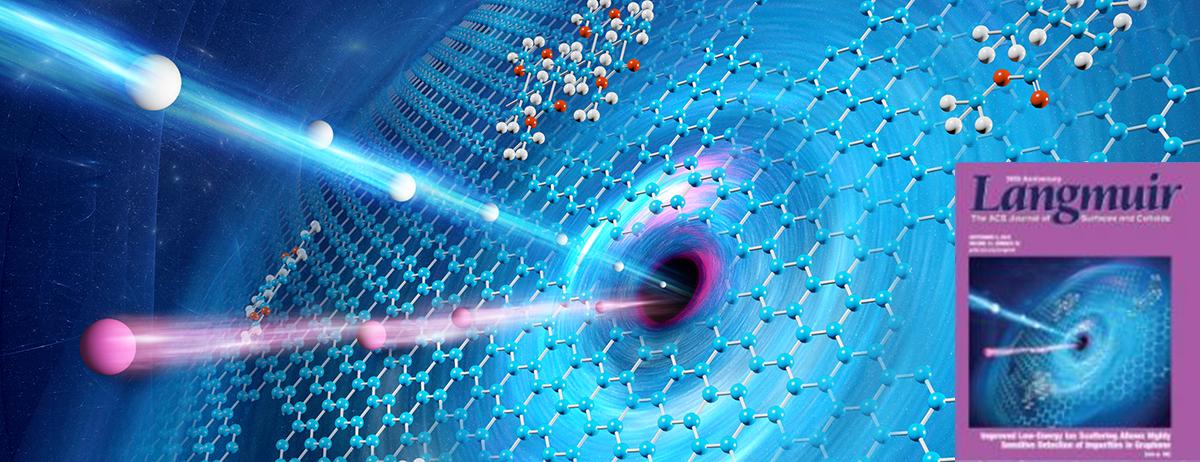
Dipolar-stabilized first and second-order antiskyrmions in ferrimagnetic multilayers
Antiskyrmions are topological spin textures with negative vorticity. Like skyrmions, they have considerable technological promise but have only been stabilised in Heusler compounds. In a recent Nature Communications article, M. Heigl et al. reports that first and second order antiskyrmions can be stabilized by dipole-dipole interaction in Fe/Gd multilayers.
The antiskyrmions and other spin textures were imaged at CEITEC Nano by Lorentz TEM at low temperature using FEI Titan system in Fresnel mode. The temperature was controlled by the Gatan Double Tilt Liquid Nitrogen Cooling Holder Model 636.
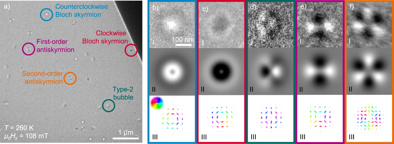
Heigl M, Koraltan S, Vaňatka M, Kraft R, Abert C, Vogler C, Semisalova A, Che P, Ullrich A, Schmidt T, Hintermayr J, Grundler D, Farle M, Urbánek M, Suess D and Albrecht M 2021 Dipolar-stabilized first and second-order antiskyrmions in ferrimagnetic multilayers Nat. Commun. 12 2611
Influence of experimental conditions on localized surface plasmon resonances measurement by electron energy loss spectroscopy
Dr Michal Horák (supervised by prof. Tomáš Šikola) has recently published in Ultramicroscopy an experimental study of the influence of the primary beam energy and the collection semi-angle on the plasmon resonances measurement by STEM-EELS. He discussed the impact on experimental characteristics which are important for successful detection of the plasmon peak in EELS, namely: the intensity of the plasmonic signal, the signal to background ratio, and the signal to zero-loss peak ratio. He found that the primary beam energy should be high enough to suppress the scattering in the sample and at the same time should be low enough to avoid the appearance of relativistic effects. Consequently, the best results are obtained using medium primary beam energy, in our case 120 keV, and an arbitrary collection semi-angle, as it is not a critical parameter at this primary beam energy.
M. Horák, T. Šikola: Influence of experimental conditions on localized surface plasmon resonances measurement by electron energy loss spectroscopy. Ultramicroscopy 216 (2020), 113044

Molecular k-Uniform tiling
Tessellation of the Euclidean plane into regular polygons – tiles – is a mathematical concept for the description of intricate geometries associated with complex structures potentially displaying unique properties. The synthetic protocols to prepare structures showing complex geometries are therefore desirable.
The multimethod approach provided by the complex UHV system of CEITEC Nano enabled the synthesis and identification of 2- and 3-uniform tilings.
Employing a combination of experimental methods (LEEM, STM, XPS), Lukáš Kormoš with his colleagues revealed that a directed chemical transformation of a 4,4’-biphenyl-dicarboxylic acid on a silver substrate results in a mixture of intact, partially, and fully chemically transformed molecules. At certain composition of the system, the molecules self-assemble into structures that can be associated with k-uniform tilings.
Nature Device and Materials Engineering Community post:
https://devicematerialscommunity.nature.com/users/384385-jan-cechal/posts/65313-kepler-would-love-it
L. Kormoš, P. Procházka, A. O. Makoveev, J. Čechal: Complex k-Uniform Tilings by a Simple Bitopic Precursor Self-Assembled on Ag(001) Surface. Nat. Commun. 11 (2020), 1856.
link: https://rdcu.be/b3FqK

Large magnetic gap at the Dirac point in Bi2Te3/MnBi2Te4 heterostructures
 New possibilities for the lossless transmission of signals, which can be used, for example, in quantum computer processors, have been tested on new compounds by an international group of scientists including experts from Masaryk University and CEITEC Nano at Brno University of Technology. New experiments with magnetically doped topological insulators, i.e. materials that conduct an electric current only on the surface and otherwise behave as insulators, were published in the renowned journal Nature.
Rienks, E. D. L.; Wimmer, S.; Sánchez-Barriga, J.; Caha, O.; Mandal, P. S.; Růžička, J.; Ney, A.; Steiner, H.; Volobuev, V. V.; Groiss, H.; Albu, M.; Kothleitner, G.; Michalička, J.; Khan, S. A.; Minár, J.; Ebert, H.; Bauer, G.; Freyse, F.; Varykhalov, A.; Rader, O.; Springholz, G.: Large magnetic gap at the Dirac point in Bi2Te3/MnBi2Te4 heterostructures, NATURE 576 (7787), p. 423-428.
We are pleased to inform you that this article "Large magnetic gap at the Dirac point in Bi2Te3/MnBi2Te4 heterostructures" is published online in Nature. Use the following SharedIt link: https://rdcu.be/b3eId
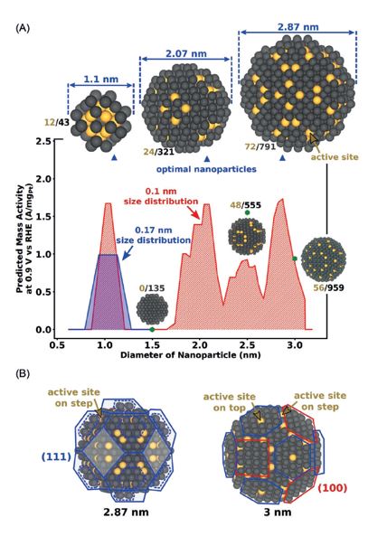
Optimizing the Size of Platinum Nanoparticles for High Oxygen Reduction Reaction Activity
The reactivity of ultra-small nanoparticles and atom precise clusters consisting of less than 50 atoms depends not only on the nanoparticle size and on the surface to volume ratio but also on the exact atomicity of the metal cluster. This has been attributed to unique cluster structures, isomers, and structural fluctuations leading to distinct electronic properties, special surface sites, and defects with altered, and even enhanced, reactivity.
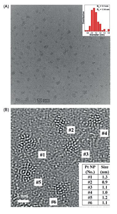
High oxygen reduction reaction (ORR) activity has been for many years considered as the key to many energy applications. By combining, theory and experiment were prepared Pt nanoparticles with the optimal size for the efficient ORR in proton-exchange-membrane fuel cells. Optimal nanoparticle sizes are predicted near 1, 2, and 3 nm by computational screening. To corroborate the computational results, it has been addressed the challenge of approximately 1 nm-sized Pt nanoparticle synthesis with a metal-organic framework (MOF) template approach.
Thanks to the capability of the aberration-corrected HR-TEM TITAN offered by the Core Facility the international team was capable to confirm the presence of atomically precise nanoclusters of atomicity near 12 and of size 1.14 ± 0.35 nm.
The authors published the results in two prestigious scientific journals, Angewandte Chemie (https://doi.org/10.1002/anie.201904492) and Journal of the American Chemical Society (https://pubs.acs.org/doi/10.1021/jacs.9b07083), where the highest to date mass activity among pure Pt catalysts for the ORR within similar size range was reported and details of synthesis and characterization of the novel MOF template containing Pt nanoclusters were described, respectively.
B. Garlyyev, K. Kratzl, M. Rück, J. Michalička, J. Fichtner, J.M. Macak, T. Kratky, S. Günther, M. Cokoja, A.S. Bandarenka, A. Gagliardi, R.A. Fischer R.A: Optimizing the Size of Platinum Nanoparticles for Enhanced Mass Activity in the Electrochemical Oxygen Reduction Reaction, Angewandte Chemie - International Edition, 58 (2019), p. 9596.
K. Kratzl, T. Kratky, S. Günther, O. Tomanec, R. Zbořil, J. Michalička, J. M. Macák, M. Cokoja, R. A. Fischer: Generation and Stabilization of Small Platinum Clusters Pt12±x Inside a Metal–Organic Framework. J. Am. Chem.Soc. 141 (2019), p. 13962.
|
|
| Figure 1: A) Predicted mass activities plotted versus nanoparticle diameters. Optimal nanoparticles (blue triangles) are identified at diameters of 1.1 nm, 2.07 nm, and 2.87 nm. B) Low-index surfaces (111) (blue) and (100) (red) depicted on the 2.87 and 3 nm nanoparticle. | Figure 2: A) Overview HR-TEM image of Pt nanoparticles and size distribution histogram (inset). B) Detailed HR-TEM image shows the magnified image of six single Pt nanoparticles and the table shows their size. |
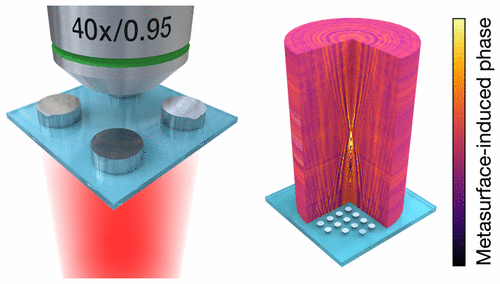
Babinet’s principle on plasmonic metasurfaces
Babinet’s principle of complementarity states that diffraction pattern from an opaque body is identical to that from a hole of the same size and shape. As plasmonic share many parallels with optics it is intriguing to explore the Babinet’s principle also in this field.
Employing large portfolio of instruments offered by Core Facility spanning from structure fabrication to optical and EELS characterization, team of V. Křápek formulated the requirements for the validity of Babinent’s principle in plasmonics.
Whereas the qualitative validity of Babinet’s principle has been confirmed, quantitative differences have been found related to the energy and quality factor of the resonances and the magnitude of related near fields.
M. Horák, V. Křápek, M. Hrtoň, A. Konečná, F. Ligmajer, M. Stöger-Pollach, T. Šamořil, A. Paták, Z. Édes, O. Metelka, J. Babocký, T. Šikola: Limits of Babinet’s principle for solid and hollow plasmonic antennas. Sci. Rep. 9 (2019), 4004.
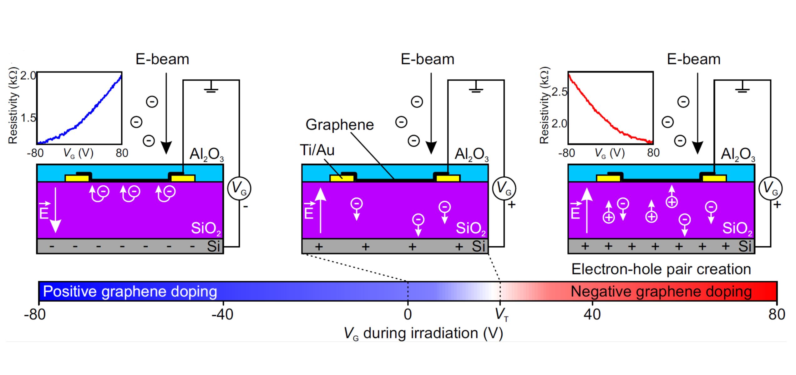
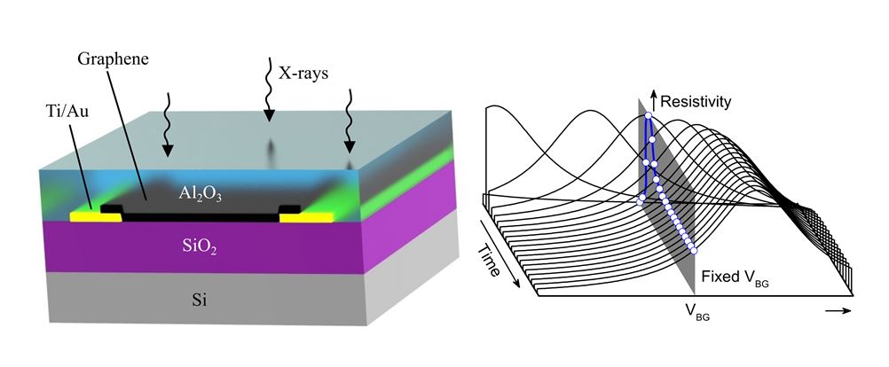
Graphene doping by electron beam
For its properties and prospective applications in many fields, graphene has attracted considerable research interest. Graphene transport properties makes graphene an attractive candidate for electronic devices, sensors, and detectors. In this context, providing graphene with controlled doping are required. One of the way, so called remote doping is based on charge trapping in gate dielectric induced by visible to X-ray radiation. However, the full-scale doping ranging from high level n-doping to high-level p-doping remained an open issue.
On devices fabricated at CF Nano Veronika Stará with her colleagues showed that low energy electron irradiation both n- and -p graphene doping can be induced.
The low-energy electron beam irradiation was employed to induce doping in a graphene layer. Authors showed that depending on the applied gate voltage during the irradiation, either n- or p-doping can be achieved, and by setting an appropriate irradiation protocol, any desired doping levels can be achieved.
V. Stará, P. Procházka, D. Mareček, T. Šikola, J. Čechal: Ambipolar Remote Graphene Doping by Low Energy Electron Beam Irradiation. Nanoscale 10, (2018), 17520.
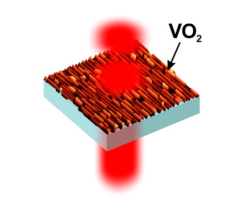
Switchable Dielectric Metasurfaces
Metasurfaces offer unparalleled functionalities for controlling the propagation and properties of electromagnetic waves. To transfer these functions to technological applications, it is critical to render them tunable and to enable fast control by external stimuli. However, the recent approaches based on top-down preparation of nanostructures are complicated and time intensive.
Based on a comprehensive analysis of epitaxial VO 2 nanostructures at CEITEC Nano Core facility, F. Ligmajer with his colleagues introduced a new class of tunable plasmonic-dielectric metasurfaces.
The epitaxial growth of VO2 on a (112̅0) face of sapphire substrate that leads to formation of a thin layer of parallel, closely spaced VO2 nanobeams. This present a promising metasurface building blocks with deeply subwavelength thickness that can be easily switched from the isotropic transparent dielectric state to the anisotropic opaque metallic state and thus effectively control the flow of light.
F. Ligmajer, L. Kejík, U. Tiwari, M. Qiu, J. Nag, M. Konečný, T. Šikola, W. Jin, R. F. Haglund, K. Appavoo, D. Y. Lei: Epitaxial VO2 Nanostructures: A Route to Large-Scale, Switchable Dielectric Metasurfaces. ACS Photonics 5 (2018), 2561.
Single-wire Nanosensor arrays
Single nanowire gas sensing devices provide better sensitivity, stability and better selectivity than bulk materials thanks to the presence of specific crystal facets offering well-defined surfaces.
On the nanoelectrode arrays featuring single nanowires fabricated at CEITEC Nano Core facility O. Chmela and coworkers showed reproducible gas sensing performance.
Employing combination of electron beam and optical lithography authors were able to manufacture platform in which single nanowires can be easily integrated by dielectrophoresis. These finding present the important step in fabrication of multifunctional sensor arrays.
O. Chmela, J. Sadílek, G. Domènech-Gil, J. Samà, J. Somer, R. Mohan, A. Romano-Rodriguez, J. Hubálek, S. Vallejos: Selectively arranged single-wire based nanosensor array systems for gas monitoring. Nanoscale 2018, 10, 9087.
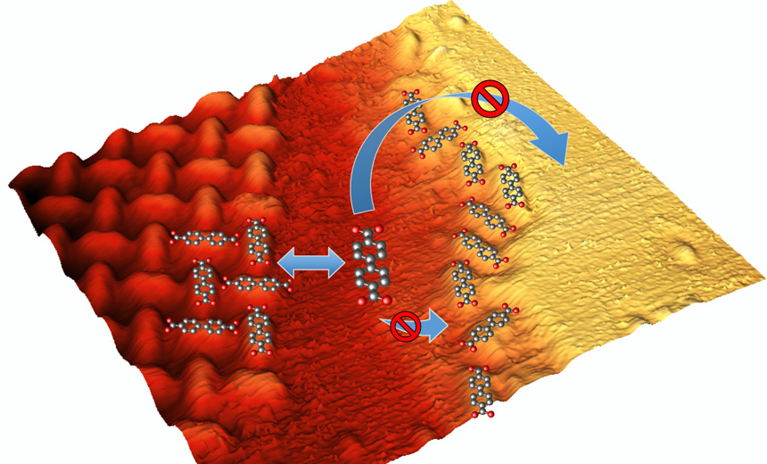
Unusual nucleation and growth
Fabrication of molecular films with a defined functionality requires the full understanding of the underlying physics. However, several molecular systems show an unusual growth behavior, for example, biphenyl dicarboxylic acid deposited on copper substrate simultaneously displays strong interaction with substrate and low interaction with substrate step edges.
A direct visualization of the system at molecular level provided by the complex UHV system of CEITEC Nano allows explaining the observed unusual growth.
Employing scanning tunneling microscopy, Lukáš Kormoš with his colleagues revealed that the strong molecular substrate interaction is even more pronounced at substrate step edges. This results in the formation of a molecular row decorating step edge, which prevents the attachment of the any further molecules there. On a mesoscopic level this is expressed as molecular repulsion from the step edges.
L. Kormoš, P. Procházka, T. Šikola, J. Čechal: Molecular Passivation of Substrate Step Edges as Origin of Unusual Growth Behavior of 4,4′-Biphenyl Dicarboxylic Acid on Cu(001), J. Phys. Chem. C 2018, 122, 2815.
Boron nitride passivation layers
Passivation of metals using protective coatings is a widespread technology and represents a huge market that generates billions of US dollars every year. 2D material offer the possibility to provide efficient protection against environment while the properties of the metal being protected are retained.
The high spatial resolution chemical analysis performed at CEITEC Nano Core facility provides insight in the mechanism of surface passivation against water and air oxidation.
The results revealed that when exposed to H2O2, a monolayer h-BN film is as inefficient as graphene as a protective coating. In contrary, 5–7 layers-thick h-BN film showed good protection, probably because of the higher resistance to transverse electron transfer from the metal to the electrolyte.
L. Jiang, N. Xiao, B. Wang, E. Grustan-Gutierrez, X. Jing, P. Bábor, M. Kolíbal, G. Lu, T. Wu, H. Wang, F. Hui, Y. Shi, B. Song, X. Xie, M. Lanza: High-resolution characterization of hexagonal boron nitride coatings exposed to aqueous and air oxidative environments, Nano Res. 2017, 10, 2046.
3D phase imaging
Phase-altering metasurfaces comprise a new class of artificial materials that allow to manipulate the wavefront of passing light and thus provide unprecedented functionalities in optics and nanophotonics.
On the metallic nanostructures fabricated at CEITEC Nano Core facility two CEITEC groups were able to perform quantitative 3D phase retrieval.
Using coherence-controlled holographic microscopy authors can obtain information about the phase of light from the whole field of view of an optical microscope in a single measurement. Quantitative 3D phase map of fabricated plasmonic zone plate shows functional phase lens with thickness below 50 nm.
J. Babocký, A. Křížová, L. Štrbková, L. Kejík, F. Ligmajer, M. Hrtoň, P. Dvořák, M. Týč, J. Čolláková, V. Křápek, R. Kalousek, R. Chmelík, T. Šikola: Quantitative 3D Phase Imaging of Plasmonic Metasurfaces, ACS Photonics 2017, 4, 1389.
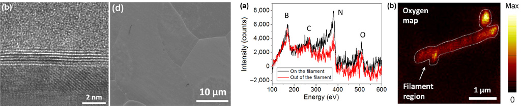
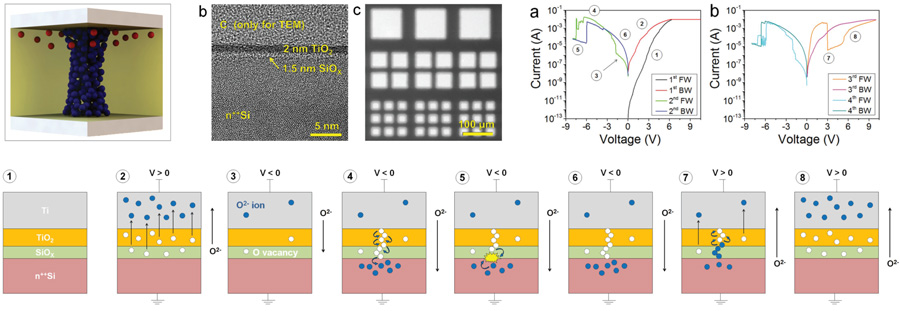
Memristive memories
Resistive random access memories (RRAM) have emerged as the flagship element allowing future massive data storage due to their excellent performance and easy fabrication. To fulfill the information storage needs of modern societies, the performance of electronic nonvolatile memories (NVMs) should be continuously improved.
The devices fabricated at CEITEC Nano Core facility show the way how to further extend the performance of RRAMs.
Ti/2-nm-TiO2/1.5-nm-SiOX/n++Si memristors exhibit unprecedented I–V characteristics with double hysteresis. This behavior is related to the coexistence of filamentary and distributed resistive switching. The simplicity of our design and the good compatibility of all the materials used (Ti, TiO2, SiOX, and n++Si), with the silicon technology give promise that these findings will be quickly implemented in real devices.
N. Xiao, M. A. Villena, B. Yuan, S. Chen, B. Wang, M. Eliáš, Y. Shi, F. Hui, X. Jing, A. Scheuermann, K. Tang, P. C. McIntyre, M. Lanza: Resistive Random Access Memory Cells with a Bilayer TiO2/SiOX Insulating Stack for Simultaneous Filamentary and Distributed Resistive Switching, Adv. Funct. Mater. 2017, 27, 1700384.
Remote Graphene doping
Graphene is a zero bandgap semiconductor. In this respect, applying external electric field it is possible to control the charge carrier type (negative or positive) and concertation in graphene, therefore to change it transport properties (e.g. resistance). This usually requires several fabrication steps, i.e. fabrication of graphene effect transistor device.
Employing the graphene devices fabricated in CEITEC Nano Core Facility Pavel Procházka and his colleagues have found that the graphene can be doped using the X-ray radiation.
In this way, the graphene properties can be remotely defined without need for any contacts. Moreover, results of the study define the framework for correct X-ray characterization of graphene and can be developed into graphene radiation sensors.
P. Procházka, D. Mareček, Z. Lišková, J. Čechal, T. Šikola: X-ray induced electrostatic graphene doping via defect charging in gate dielectric, Sci. Rep. 7 (2017), 563.
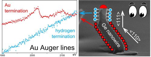
Nano Letters article
Mira Kolíbal used NanoSAM at CEITEC Nano to reveal the essential role of atomic hydrogen in determining the growth direction of Ge nanowires with an Au catalyst.
M. Kolíbal, T. Pejchal, T. Vystavěl, T. Šikola: The synergic effect of atomic hydrogen adsorption and catalyst spreading on Ge nanowire growth orientation and kinking, Nano Lett. 16 (8), (2016), 4880–4886.
ACS Editors Choice and Cover
The paper resulting from work on TOF-SIMS QTAC by Stan Průša, Pavel Procházka, Petr Bábor, Tomáš Šikola and their coworkers was chosen by Langmuir editor as the Editors choice!
S. Průša, P. Procházka, P. Bábor, T. Šikola, R. ter Veen, M. Fartmann, T. Grehl , P. Brüner, D. Roth, P. Bauer, H. H. Brongersm: Highly Sensitive Detection of Surface and Intercalated Impurities in Graphene by LEIS, Langmuir 31 (2015), 9628.