
CEITEC Nano Research Infrastructure
Brno University of Technology
Purkyňova 123, 612 00 Brno
Czech Republic
 +420 54114 9207
 nano@ceitec.vutbr.cz
Consumables | wh | ShP | i | feedback


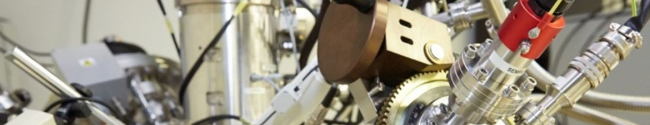
Focused Ion Beam/Scanning Electron Microscope FEI Helios NanoLab 660 (HELIOS)

Guarantor:
Ondřej Man, Ph.D.
Instrument status:
![]() Operational, 20.5.2025 12:39
Operational, 20.5.2025 12:39
Equipment placement:
CEITEC Nano - A1.10
FEG-type scanning electron microscope with High/Low vacuum regime with resolution at least 1,5 nm @ 15 kV (in high vacuum mode) and with chamber allowing XY stage travel at least 100x100 mm. Equipped with analytical attachments EDS + WDS + EBSD.
Publications:
-
Huang, Y.; Chen, Z.; Meindlhumer, M.; Hahn, R.; Holec, D.; Leiner, T.; Maier-Kiener, V.; Zheng, Y.; Zhang, Z.; Hatzenbichler, L.; Riedl, H.; Mitterer, C.; Zhang, Z., 2025: Harvesting superior intrinsic plasticity in nitride ceramics with negative stacking fault energy. ACTA MATERIALIA 286(286), p. 1 - 15, doi: 10.1016/j.actamat.2025.120774; FULL TEXT
(TITAN, HELIOS) -
TRUNEC, M.; ŠŤASTNÝ, P.; ŠIŠKA VIRÁGOVÁ, E.; SOBOLA, D., 2025: Pore coalescence as an inherent problem in the sintering of zirconia nanoparticles. JOURNAL OF THE EUROPEAN CERAMIC SOCIETY 45(8), doi: 10.1016/j.jeurceramsoc.2025.117272; FULL TEXT
(VERIOS, HELIOS, TITAN, KRATOS-XPS, RIGAKU3) -
Tichý, M., 2024: In-situ analysis of magnetic phase transition in FeRh using transmission electron microscopy. BACHELOR´S THESIS , p. 1 - 48; FULL TEXT
(VERSALAB, HELIOS, TITAN) -
Štindl, J., 2024: Correlative imaging of magnetic order in antiferromagnets. BACHELOR´S THESIS , p. 1 - 44; FULL TEXT
(VERSALAB, KERR-MICROSCOPE, HELIOS, SAW-ACCUTOM, US-CUTTER, TITAN) -
Gazdík, R., 2024: Defect localization and analysis in GaN. MASTER´S THESIS , p. 1 - 66; FULL TEXT
(MIRA-STAN, HELIOS, TITAN)
-
Karpinski, D.; Polcar, T.; Bondarev, A., 2024: Exploring nanoscale metallic multilayer Ta/Cu films: Structure and some insights on deformation and strengthening mechanisms. MATERIALS CHARACTERIZATION 212, doi: 10.1016/j.matchar.2024.113933; FULL TEXT
(TITAN, VERIOS, HELIOS) -
ZIEGELWANGER, T.; REISINGER, M.; MATOY, K.; MEDJAHED, A.; ZÁLEŠÁK, J.; GRUBER, M.; MEINDLHUMER, M.; KECKES, J., 2024: Backside metallization affects residual stress and bending strength of the recast layer in laser-diced Si. MATERIALS SCIENCE IN SEMICONDUCTOR PROCESSING 181, p. 1 - 11, doi: 10.1016/j.mssp.2024.108579; FULL TEXT
(HELIOS, TITAN) -
Foltýn, M., 2024: Plasmonics of non-noble metals. MASTER´S THESIS , p. 1 - 83; FULL TEXT
(HELIOS, MAGNETRON, TITAN, RIGAKU3, LITESCOPE-MIRA-STAN) -
FOLTÝN, M.; PATOČKA, M.; ŘEPA, R.; ŠIKOLA, T.; HORÁK, M., 2024: Influence of Deposition Parameters on the Plasmonic Properties of Gold Nanoantennas Fabricated by Focused Ion Beam Lithography. ACS OMEGA 9(35), p. 37408 - 9, doi: 10.1021/acsomega.4c06598; FULL TEXT
(TITAN, HELIOS, RIGAKU3, LITESCOPE-MIRA-STAN) -
ČALKOVSKÝ, V.; MACH, J.; BARTOŠÍK, M.; PIASTEK, J.; KOSTKA, M.; MIKERÁSEK, V.; SUPALOVÁ, L.; KONEČNÝ, M.; KVAPIL, M.; HORÁK, M.; ŠIKOLA, T., 2024: Preparation of GaN Nanocrystals with Single Ag Cores. CRYSTAL GROWTH AND DESIGN 24(19), p. 7904 - 6, doi: 10.1021/acs.cgd.4c00776; FULL TEXT
(TITAN, HELIOS, TERS) -
Zeman, P.; Haviar, S.; Houška, J.; Thakur, D.; Bondarev, A.; Červená, M.; Medlín, R.; Čerstvý, R., 2024: Self-formation of dual-phase nanocomposite Zr–Cu–N coatings based on nanocrystalline ZrN and glassy ZrCu. MATERIALS & DESIGN 245, doi: 10.1016/j.matdes.2024.113278; FULL TEXT
(TITAN, HELIOS, NANOINDENTER) -
Antunes Corrêa, C.; Volný, J.; Uhlířová, K.; Verhagen, T., 2024: Mapping Sliding Ferroelectricity in Bulk (PbS) 1.11 VS 2 Crystals. PHYSICA STATUS SOLIDI (RRL) – RAPID RESEARCH LETTERS 18(12), p. 1 - 8, doi: 10.1002/pssr.202400189; FULL TEXT
(TITAN, HELIOS) -
SEPÚLVEDA SEPÚLVEDA, L.; SOPHA, H.; NORIKAWA, Y.; HROMÁDKO, L.; RODRIGUEZ PEREIRA, J.; MAN, O.; NOHIRA, T.; YASUDA, K.; MACÁK, J., 2024: Can electrodeposited Ti replace rolled Ti as substrate for the growth of anodic TiO2 nanotube layers?. ELECTROCHIMICA ACTA 479, doi: 10.1016/j.electacta.2024.143877; FULL TEXT
(HELIOS) -
Frank, F.; Tkadletz, M.; Saringer, C.; Czettl, C.; Pohler, M.; Burghammer, M.; Todt, J.; Zalesak, J.; Keckes, J.; Schalk, N., 2023: Investigation of the microstructure of a graded ZrN/Ti0.33Al0.67N multilayer coating using cross-sectional characterization methods. SURFACE AND COATINGS TECHNOLOGY 453, p. 1 - 8, doi: 10.1016/j.surfcoat.2022.129126; FULL TEXT
(HELIOS, TITAN) -
Kuptsov, K.A.; Antonyuk, M.N.; Sheveyko, A.N.; Bondarev, A.V.; Ignatov, S.G.; Slukin, P.V.; Dwivedi, P.; Fraile, A.; Polcar, T.; Shtansky, D.V., 2023: High-entropy Fe-Cr-Ni-Co-(Cu) coatings produced by vacuum electro-spark deposition for marine and coastal applications. SURFACE AND COATINGS TECHNOLOGY 453, doi: 10.1016/j.surfcoat.2022.129136; FULL TEXT
(TITAN, HELIOS) -
Kuptsov, K. A.; Antonyuk, M. N.; Sheveyko, A. N.; Bondarev, A. V.; Shtansky, D. V., 2023: Influence of TiC Addition on Corrosion and Tribocorrosion Resistance of Cr2Ti-NiAl Electrospark Coatings. COATINGS 13(2), doi: 10.3390/coatings13020469; FULL TEXT
(TITAN, HELIOS, NANOINDENTER) -
ZANGANA, S.; LEDNICKÝ, T.; BONYÁR, A., 2023: Three Generations of Surface Nanocomposites Based on Hexagonally Ordered Gold Nanoparticle Layers and Their Application for Surface-Enhanced Raman Spectroscopy. CHEMOSENSORS 11(4), p. 1 - 14, doi: 10.3390/chemosensors11040235; FULL TEXT
(VERIOS, HELIOS, RIE-FLUORINE, DIENER) -
ŠŤASTNÝ, P.; CHLUP, Z.; HLINIČAN, J.; KAŠTYL, J.; TRUNEC, M., 2023: Effect of cyclic loading on the microstructure of thin zirconia tapes. JOURNAL OF THE EUROPEAN CERAMIC SOCIETY 43(10), p. 4498 - 8, doi: 10.1016/j.jeurceramsoc.2023.03.024; FULL TEXT
(VERIOS, HELIOS, LEICACOAT-STAN, RIGAKU3, WITEC-RAMAN) -
ARREGI URIBEETXEBARRIA, J.; RINGE, F.; HAJDUČEK, J.; GOMONAY, O.; MOLNÁR, T.; JASKOWIEC, J.; UHLÍŘ, V., 2023: Magnetic-field-controlled growth of magnetoelastic phase domains in FeRh. JOURNAL OF PHYSICS: MATERIALS 6(3), p. 1 - 15, doi: 10.1088/2515-7639/acce6f; FULL TEXT
(MAGNETRON, KERR-MICROSCOPE, VERSALAB, RIGAKU9, ICON-SPM, HELIOS, TITAN) -
POLAT, Ö.; HORÁK, M.; ARREGI URIBEETXEBARRIA, J.; BUKVIŠOVÁ, K.; ZLÁMAL, J.; ŠIKOLA, T., 2023: Synthesis and characterization of half-Heusler ScPtBi films via three-source magnetron co-sputtering on Nb superconductor buffer layer. SURFACES AND INTERFACES 40, doi: 10.1016/j.surfin.2023.103118; FULL TEXT
(MAGNETRON, RIGAKU9, TITAN, HELIOS, KRATOS-XPS, CRYOGENIC, LYRA) -
Mouralova, K.; Bednar, J.; Benes, L.; Polzer, A.; Zahradnicek, R.; Fries, J.; Prokes, T., 2023: Machining of 1.2363 and 1.2343ESR steels using EDM. JOURNAL OF THE BRAZILIAN SOCIETY OF MECHANICAL SCIENCES AND ENGINEERING 45(7), doi: 10.1007/s40430-023-04293-9; FULL TEXT
(DEKTAK, LYRA, TITAN, HELIOS, TEGRAMIN) -
Bondarev, A.; Al-Rjoub, A.; Bin Yaqub, T.; Polcar, T.; Fernandes, F., 2023: TEM study of the oxidation resistance and diffusion processes in a multilayered TiSiN/TiN(Ag) coating designed for tribological applications. APPLIED SURFACE SCIENCE 609, doi: 10.1016/j.apsusc.2022.155319; FULL TEXT
(HELIOS, TITAN) -
HORÁK, M.; KONEČNÁ, A.; ŠIKOLA, T.; KŘÁPEK, V., 2023: Spatio-spectral metrics in electron energy loss spectroscopy as a tool to resolve nearly degenerate plasmon modes in dimer plasmonic antennas. NANOPHOTONICS 12(15), p. 3089 - 10, doi: 10.1515/nanoph-2023-0153; FULL TEXT
(MAGNETRON, HELIOS, TITAN) -
Bondarev, A.; Simonovic, K.; Vitu, T.; Kožmín, P.; Syrovatka, Š.; Polcar, T., 2023: Textured coating or coated texture: Femtosecond laser texturing of a-C:H/WC coatings for dry friction applications. SURFACE AND COATINGS TECHNOLOGY 469, doi: 10.1016/j.surfcoat.2023.129808; FULL TEXT
(HELIOS, KRATOS-XPS, MIRA-STAN) -
Riley, J. A.; Horák, M.; Křápek, V.; Healy, N.; Pacheco-Peña, V., 2023: Plasmonic sensing using Babinet´s principle. NANOPHOTONICS , doi: 10.1515/nanoph-2023-0317; FULL TEXT
(LEICACOAT-STAN, HELIOS, TITAN) -
PONGRÁCZ, J.; VACEK, P.; GRÖGER, R., 2023: Recombination activity of threading dislocations in MOVPE-grown AlN/Si {111} films etched by phosphoric acid. JOURNAL OF APPLIED PHYSICS 134(19), doi: 10.1063/5.0171937; FULL TEXT
(LYRA, ICON-SPM, HELIOS, TITAN, LEICACOAT-NANO) -
ALFREIDER, M.; MEINDLHUMER, M.; ZIEGELWANGER, T.; DANIEL, R.; KECKES, J.; KIENER, D., 2023: Revealing dynamic-mechanical properties of precipitates in a nanostructured thin film using micromechanical spectroscopy. MRS BULLETIN 49(1), p. 49 - 10, doi: 10.1557/s43577-023-00549-w; FULL TEXT
(HELIOS, TITAN) -
POLAT, Ö.; ARREGI URIBEETXEBARRIA, J.; HORÁK, M.; POLČÁK, J.; BUKVIŠOVÁ, K.; ZLÁMAL, J.; ŠIKOLA, T., 2022: The fabrication and characterization of half-Heusler YPdBi thin films. JOURNAL OF PHYSICS AND CHEMISTRY OF SOLIDS 161, p. 1 - 6, doi: 10.1016/j.jpcs.2021.110447; FULL TEXT
(MAGNETRON, RIGAKU9, TITAN, HELIOS, KRATOS-XPS, CRYOGENIC, LYRA) -
Gsellmann, M.; Scheiber, D.; Klünsner, T.; Zálešák, J;. Zhang, Z.; Leitner, H.; Mitterer, C.; Ressel, G.; Romaner, L., 2022: Bond strength between TiN coating and microstructural constituents of a high speed steel determined by first principle calculations. ACTA MATERIALIA 222, p. 1 - 9, doi: 10.1016/j.actamat.2021.117439; FULL TEXT
(HELIOS, TITAN) -
HORKÝ, M.; ARREGI URIBEETXEBARRIA, J.; PATEL, S.; STAŇO, M.; MEDAPALLI, R.; CAHA, O.; VOJÁČEK, L.; HORÁK, M.; UHLÍŘ, V.; FULLERTON, E., 2022: Controlling the Metamagnetic Phase Transition in FeRh/MnRh Superlattices and Thin-Film Fe50-xMnxRh50 Alloys. ACS APPLIED MATERIALS & INTERFACES 14(2), p. 3568 - 12, doi: 10.1021/acsami.1c22460; FULL TEXT
(VERSALAB, RIGAKU9, HELIOS, TITAN, ICON-SPM) -
Polzer, A.; Mouralova, K.; Benes, L.; Zahradnicek, R.; Fries, J., 2022: Comparison of machinability of nickel alloys using WEDM. PROCEEDINGS OF THE INSTITUTION OF MECHANICAL ENGINEERS, PART B: JOURNAL OF ENGINEERING MANUFACTURE , doi: 10.1177/09544054221075876; FULL TEXT
(TEGRAMIN, DEKTAK, HELIOS, TITAN, LYRA) -
Stückler, M.; Zálešák, J.; Müller, T.; Wurster, S.; Weissitsch, L.; Meier, M.; Felfer, P.; Gammer, C.; Pippan, R.; Bachmaier, A., 2022: Oxide-stabilized microstructure of severe plastically deformed CuCo alloys. JOURNAL OF ALLOYS AND COMPOUNDS 901, p. 163616-1 - 11, doi: 10.1016/j.jallcom.2022.163616; FULL TEXT
(HELIOS, TITAN) -
PISARENKO, T.; PAPEŽ, N.; SOBOLA, D.; ŢĂLU, Ş.; ČÁSTKOVÁ, K.; ŠKARVADA, P.; MACKŮ, R.; ŠČASNOVIČ, E.; KAŠTYL, J., 2022: Comprehensive characterization of PVDF nanofibers at macro- and nanolevel. POLYMERS 14(3), p. 593 - 18, doi: 10.3390/polym14030593; FULL TEXT
(HELIOS, WITEC-RAMAN, FTIR-CHEMLAB, KRATOS-XPS, SEE-SYSTEM, LYRA) -
KAŠTYL, J.; ŠŤASTNÝ, P.; CHLUP, Z.; SONG, L.; ŠČASNOVIČ, E.; TRUNEC, M., 2022: Gelcast zirconia ceramics for dental applications combining high strength and high translucency. JOURNAL OF THE AMERICAN CERAMIC SOCIETY 105(6), p. 3909 - 16, doi: 10.1111/jace.18417; FULL TEXT
(VERIOS, TITAN, HELIOS, RIGAKU3, DEKTAK, WITEC-RAMAN) -
ZHU, K.; MAHMOODI, M.; FAHIMI, Z.; XIAO, Y.; WANG, T.; BUKVIŠOVÁ, K.; KOLÍBAL, M.; ROLDÁN, J.; PEREZ, D.; AGUIRRE, F.; LANZA, M., 2022: Memristors with Initial Low-Resistive State for Efficient Neuromorphic Systems. ADVANCED INTELLIGENT SYSTEMS , p. 2200001 - 9, doi: 10.1002/aisy.202200001; FULL TEXT
(TITAN, HELIOS) -
PEJCHAL, T.; BUKVIŠOVÁ, K.; VALLEJOS VARGAS, S.; CITTERBERG, D.; ŠIKOLA, T.; KOLÍBAL, M., 2022: Ga interaction with ZnO surfaces: Diffusion and melt-back etching. APPLIED SURFACE SCIENCE 583, p. 152475 - 6, doi: 10.1016/j.apsusc.2022.152475; FULL TEXT
(WITEC-RAMAN, UHV-DEPOSITION, UHV-PREPARATION, NANOSAM, VERIOS, KRATOS-XPS, HELIOS) -
Krizek, F.; Reimers, S.; Kaspar, Z.; Marmodoro, A.; Michalicka, J.; Man, O.; Edstrom, A.; Amin, OJ.; Edmonds, KW.; Campion, RP.; Maccherozzi, F. ; Dhesi, SS.; Zubac, J.; Kriegner, D.; Carbone, D.; Zelezny, J. ; Vyborny, K.; Olejnik, K.; Novak, V.; Rusz, J.; Idrobo, JC.; Wadley, P.; Jungwirth, T., 2022: Atomically sharp domain walls in an antiferromagnet. SCIENCE ADVANCES 8(13), p. eabn3535-1 - 10, doi: 10.1126/sciadv.abn3535; FULL TEXT
(TITAN, LEICACOAT-STAN, HELIOS) -
POLAT, Ö.; MOHELSKÝ, I.; ARREGI URIBEETXEBARRIA, J.; HORÁK, M.; POLČÁK, J.; BUKVIŠOVÁ, K.; ZLÁMAL, J.; ŠIKOLA, T., 2022: An investigation of structural and magnetotransport features of half-Heusler ScPtBi thin films. MATERIALS RESEARCH BULLETIN 149, p. 111696-1 - 7, doi: 10.1016/j.materresbull.2021.111696; FULL TEXT
(MAGNETRON, RIGAKU9, TITAN, HELIOS, KRATOS-XPS, CRYOGENIC, LYRA) -
Plichta, T.; Zahradnicek, R.; Cech, V., 2022: Surface topography affects the nanoindentation data. THIN SOLID FILMS 745, doi: 10.1016/j.tsf.2022.139105; FULL TEXT
(HELIOS, NANOINDENTER) -
Kutzhanov, M. K.; Matveev, A. T.; Bondarev, A. V.; Polcar, T.; Duchoň, J.; Shtansky, D. V., 2022: Al-based composites reinforced with ceramic particles formed by in situ reactions between Al and amorphous SiNxOy. MATERIALS SCIENCE AND ENGINEERING: A 842, doi: 10.1016/j.msea.2022.143105; FULL TEXT
(TITAN, HELIOS) -
Corthay, S.; Kutzhanov, M. K.; Matveev, A. T.; Bondarev, A. V.; Leybo, D. V.; Shtansky, D. V., 2022: Nanopowder derived Al/h-BN composites with high strength and ductility. JOURNAL OF ALLOYS AND COMPOUNDS 912, doi: 10.1016/j.jallcom.2022.165199; FULL TEXT
(HELIOS, TITAN) -
Sreedhara, MB.; Bukvisova, K.; Khadiev, A.; Citterberg, D.; Cohen, H.; Balema, V.; Pathak, AK.; Novikov, D.; Leitus, G.; Kaplan-Ashiri, I.; Kolibal, M.; Enyashin, AN.; Houben, L.; Tenne, R., 2022: Nanotubes from the Misfit Layered Compound (SmS)(1.)19TaS2: Atomic Structure, Charge Transfer, and Electrical Properties. CHEMISTRY OF MATERIALS 34(4), p. 1838 - 16, doi: 10.1021/acs.chemmater.1c04106; FULL TEXT
(TITAN, HELIOS, RAITH, EVAPORATOR, MPS150, KEITHLEY-4200, ALD) -
Karner, S.; Blank, O.; Rösch, M.; Burghammer, M.; Zalesak, J.; Keckes, J.; Todt, J., 2022: X-ray nanodiffraction analysis of residual stresses in polysilicon electrodes of vertical power transistors. MATERIALIA 24, p. 101484-1 - 6, doi: 10.1016/j.mtla.2022.101484; FULL TEXT
(HELIOS) -
TRUNEC, M.; ŠŤASTNÝ, P.; KAŠTYL, J., 2022: Defect-free drying of large fine-particle zirconia compacts prepared by gelcasting method. JOURNAL OF THE EUROPEAN CERAMIC SOCIETY 42(15), p. 7180 - 7, doi: 10.1016/j.jeurceramsoc.2022.08.011; FULL TEXT
(HELIOS) -
PRADHAN, G.; CELEGATO, F.; BARRERA, G.; OLIVETTI, E.S.; COISSON, M.; HAJDUČEK, J.; ARREGI URIBEETXEBARRIA, J.; ČELKO, L.; UHLÍŘ, V.; RIZZI, P.; TIBERTO, P., 2022: Magnetic properties of FeGa/Kapton for flexible electronics. SCIENTIFIC REPORTS 12(1), p. 17503 - 11, doi: 10.1038/s41598-022-21589-3; FULL TEXT
(HELIOS, TITAN, KERR-MICROSCOPE) -
SCHMIDT, N.; ABDULAZHANOV, S.; MICHALIČKA, J.; HINTERMAYR, J.; MAN, O.; CAHA, O.; URBÁNEK, M.; ALBRECHT, M., 2022: Effect of Gd addition on the structural and magnetic properties of L1(0)-FePt alloy thin films. JOURNAL OF APPLIED PHYSICS 132(21), doi: 10.1063/5.0124652; FULL TEXT
(TITAN, HELIOS, RIGAKU9) -
ŠŤASTNÝ, P.; SMIEŠKOVÁ, J.; TRUNEC, M., 2022: Preparation of multilayer ceramic tapes by aqueous gel-tape co-casting. CERAMICS INTERNATIONAL 48(21), p. 32546 - 5, doi: 10.1016/j.ceramint.2022.07.248; FULL TEXT
(HELIOS, VERIOS) -
Demelius, L.; Blatnik, M.; Unger, K.; Parlanti, P.; Gemmi, M.; Coclite, A.M., 2022: Shedding light on the initial growth of ZnO during plasma-enhanced atomic layer deposition on vapor-deposited polymer thin films. APPLIED SURFACE SCIENCE 604, p. 1 - 13, doi: 10.1016/j.apsusc.2022.154619; FULL TEXT
(HELIOS, KRATOS-XPS) -
Bondarev, A.; Ponomarev, I.; Muydinov, R.; Polcar, T., 2022: Friend or Foe? Revising the Role of Oxygen in the Tribological Performance of Solid Lubricant MoS2. ACS APPLIED MATERIALS AND INTERFACES 14(49), p. 55051 - 55061, doi: 10.1021/acsami.2c15706; FULL TEXT
(HELIOS, TITAN, KRATOS-XPS, VERIOS, MIRA-STAN) -
Holobrádek, J., 2022: Low damping magnonic (meta)materials with enhanced control over local magnetic properties. TREATISE TO STATE DOCTORAL EXAM , p. 1 - 26
(VERIOS, HELIOS, KERR-MICROSCOPE, MAGNETRON, KAUFMAN) -
Kamnev, K., 2022: Porous-alumina-assisted formation of metal and metal-oxide nanostructures for use in advanced micro-devices. PH.D. THESIS , p. 1 - 145; FULL TEXT
(VERIOS, HELIOS, TITAN, MAGNETRON, MPS150, KEITHLEY-4200) -
Turčan, I., 2022: Magnetism in curved geometries. PH.D. THESIS , p. 1 - 117; FULL TEXT
(LYRA, BRILLOUIN, ICON-SPM, MIRA-EBL, KERR-MICROSCOPE, HELIOS) -
Hudec, T.; Izai, V.; Satrapinskyy, L.; Huminiuc, T.; Roch, T.; Gregor, M.; Grančič, B.; Mikula, M.; Polcar, T., 2021: Structure, mechanical and tribological properties of MoSe2 and Mo-Se-N solid lubricant coatings. SURFACE AND COATINGS TECHNOLOGY 405, doi: 10.1016/j.surfcoat.2020.126536
(TITAN, HELIOS) -
IMRICH, T.; ZAZPE MENDIOROZ, R.; KRÝSOVÁ, H.; PAUŠOVÁ, Š.; DVOŘÁK, F.; RODRIGUEZ PEREIRA, J.; MICHALIČKA, J.; MAN, O.; MACÁK, J.; NEUMANN-SPALLART, M.; KRÝSA, J., 2021: Protection of hematite photoelectrodes by ALD-TiO2 capping. JOURNAL OF PHOTOCHEMISTRY AND PHOTOBIOLOGY A:CHEMISTRY 409, p. 113126-1 - 7, doi: 10.1016/j.jphotochem.2020.113126; FULL TEXT
(TITAN, HELIOS) -
ŘIHÁČEK, T.; HORÁK, M.; SCHACHINGER, T.; MIKA, F.; MATĚJKA, M.; KRÁTKÝ, S.; FOŘT, T.; RADLIČKA, T.; JOHNSON, C.; NOVÁK, L.; SEĎA, B.; MCMORRAN, B.; MÜLLEROVÁ, I., 2021: Beam shaping and probe characterization in the scanning electron microscope. ULTRAMICROSCOPY 225, p. 1 - 9, doi: 10.1016/j.ultramic.2021.113268; FULL TEXT
(HELIOS, LEICACOAT-STAN) -
Hlushko, K.; Mackova, A.; Zalesak, J.; Burghammer, M.; Davydok, A.; Krywka, C.; Daniel, R.; Keckes, J.; Todt, J., 2021: Ion irradiation-induced localized stress relaxation in W thin film revealed by cross-sectional X-ray nanodiffraction. THIN SOLID FILMS 722, doi: 10.1016/j.tsf.2021.138571
(HELIOS) -
Bondarev, A. V.; Antonyuk, M. N.; Kiryukhantsev-Korneev, Ph V.; Polcar, T.; Shtansky, D. V., 2021: Insight into high temperature performance of magnetron sputtered Si-Ta-C-(N) coatings with an ion-implanted interlayer. APPLIED SURFACE SCIENCE 541, doi: 10.1016/j.apsusc.2020.148526; FULL TEXT
(VERIOS, HELIOS, KRATOS-XPS, NANOINDENTER) -
Hajduček, J., 2021: Imaging of metamagnetic thin films using TEM. MASTER´S THESIS , p. 1 - 78; FULL TEXT
(MAGNETRON, VERSALAB, MIRA-EBL, HELIOS, TITAN) -
ZÁLEŠÁK, J.; TODT, J.; MICHALIČKA, J.; SARTORY, B.; MATKO, I.; LESSIAK, M.; TRAXLER, M.; WEISSENBACHER, R.; PITON, R.; GAMMER, C.; KECKES, J., 2021: Effect of Pressure and Temperature on Microstructure of Self-Assembled Gradient AlxTi1-xN Coatings. COATINGS, MDPI 11(4), p. 416-1 - 15, doi: 10.3390/coatings11040416; FULL TEXT
(HELIOS, TITAN) -
Vitu, T.; Huminiuc, T.; Doll, G.; Bousser, E.; Matthews, A.; Polcar, T., 2021: Tribological properties of Mo-S-C coating deposited by pulsed d.c. magnetron sputtering. WEAR 480-481, doi: 10.1016/j.wear.2021.203939; FULL TEXT
(HELIOS) -
Piatková, B., 2021: Isolation of Sceletium tortuosum compounds with a possible antidepressant activity. MASTER´S THESIS , p. 1 - 99; FULL TEXT
(HELIOS) -
Mouralova, K.; Polzer, A.; Benes, L.; Bednar, J.; Zahradnicek, R.; Prokes, T.; Fiala, Z.; Fries, J., 2021: Machining of B1914 nickel-based superalloy using wire electrical discharge machining. PROCEEDINGS OF THE INSTITUTION OF MECHANICAL ENGINEERS, PART E: JOURNAL OF PROCESS MECHANICAL ENGINEERING , doi: 10.1177/09544089211031746; FULL TEXT
(TEGRAMIN, DEKTAK, HELIOS, TITAN, LYRA) -
ORUDZHEV, F.; RAMAZANOV, S.; SOBOLA, D.; KASPAR, P.; TRČKA, T.; ČÁSTKOVÁ, K.; KAŠTYL, J.; ZVEREVA, I.; WANG, C.; SELIMOV, D.; GULAKHMEDOV, R.; ABDURAKHMANOV, M.; SHUAIBOV, A.; KADIEV, M., 2021: Ultrasound and water flow driven piezophototronic effect in self-polarized flexible alpha-Fe2O3 containing PVDF nanofibers film for enhanced catalytic oxidation. NANO ENERGY 90, p. 1 - 13, doi: 10.1016/j.nanoen.2021.106586; FULL TEXT
(FTIR, KRATOS-XPS, HELIOS, JAZ3-CHANNEL, LEICACOAT-STAN, WITEC-RAMAN) -
Polzer, A.; Sedlak, J.; Sedlacek, J.; Benes, L.; Mouralova, K., 2021: Vertical graphene growth on AlCu4Mg alloy by PECVD technique. COATINGS 11(9), doi: 10.3390/coatings11091108; FULL TEXT
(PECVD-NANOFAB, TITAN, HELIOS, ICON-SPM) -
TURČAN, I.; FLAJŠMAN, L.; WOJEWODA, O.; ROUČKA, V.; MAN, O.; URBÁNEK, M., 2021: Spin wave propagation in corrugated waveguides. APPLIED PHYSICS LETTERS 118(9), p. 1 - 5, doi: 10.1063/5.0041138; FULL TEXT
(HELIOS, RAITH, KERR-MICROSCOPE, VERSALAB, VNA-MPI, BRILLOUIN, LYRA, ICON-SPM) -
Mouralova, K.; Polzer, A.; Benes, L.; Bednar, J.; Zahradnicek, R.; Kalivoda, M.; Fries, J., 2021: Multicut technology used in WEDM machining of Mar-M247. PROCEEDINGS OF THE INSTITUTION OF MECHANICAL ENGINEERS, PART B: JOURNAL OF ENGINEERING MANUFACTURE , doi: 10.1177/09544054211043484; FULL TEXT
(DEKTAK, TEGRAMIN, HELIOS, TITAN, LYRA) -
KAMNEV, K.; SEPÚLVEDA SEPÚLVEDA, L.; BENDOVÁ, M.; PYTLÍČEK, Z.; PRÁŠEK, J.; KOLÍBALOVÁ, E.; MICHALIČKA, J.; MOZALEV, A., 2021: The Growth, Composition, and Functional Properties of Self-Organized Nanostructured ZrO2-Al2O3 Anodic Films for Advanced Dielectric Applications. MATERIALS CHEMISTRY FRONTIERS 7(10), p. 1 - 13, doi: 10.1002/aelm.202100505; FULL TEXT
(TITAN, MAGNETRON, HELIOS, VERIOS) -
Kuptsov, K. A.; Antonyuk, M. N.; Bondarev, A. V.; Sheveyko, A. N.; Shtansky, D. V., 2021: Electrospark deposition of wear and corrosion resistant Ta(Zr)C-(Fe,Mo,Ni) coatings to protect stainless steel from tribocorrosion in seawater. WEAR 486-487, doi: 10.1016/j.wear.2021.204094; FULL TEXT
(TITAN, HELIOS) -
Černohorský, P.; Pisarenko, T.; Papež, N.; Sobola, D.; Ţălu, Ş.; Částková, K.; Kaštyl, J.; Macků, R.; Škarvada, P.; Sedlák, P., 2021: Structure Tuning and Electrical Properties of Mixed PVDF and Nylon Nanofibers. MATERIALS 14(20), doi: 10.3390/ma14206096; FULL TEXT
(FTIR, WITEC-RAMAN, KRATOS-XPS, HELIOS, LEICACOAT-STAN, SEE-SYSTEM, LYRA) -
Hudec, T.; Bondarev, A.; Izai, V.; Šroba, V.; Satrapinskyy, L.; Roch, T.; Turiničová, V.; Grančič, B.; Polcar, T.; Mikula, M., 2021: Titanium doped MoSe2 coatings – Synthesis, structure, mechanical and tribological properties investigation. APPLIED SURFACE SCIENCE 568, doi: 10.1016/j.apsusc.2021.150990; FULL TEXT
(TITAN, HELIOS) -
Daniel, R.; Zalesak, J.; Matko, I.; Baumegger, W.; Hohenwarter, A.; George, E. P.; Keckes, J., 2021: Microstructure-dependent phase stability and precipitation kinetics in equiatomic CrMnFeCoNi high-entropy alloy: Role of grain boundaries. ACTA MATERIALIA 223, p. 117470-1 - 8, doi: 10.1016/j.actamat.2021.117470; FULL TEXT
(TITAN, HELIOS) -
Pejchal, T., 2021: Towards highly-doped Ge and ZnO nanowires: Growth, characterization and doping level analysis. PH.D. THESIS ; FULL TEXT
(NANOSAM, WITEC-RAMAN, UHV-DEPOSITION, UHV-PREPARATION, VERIOS, KRATOS-XPS, HELIOS, TITAN, ALD, EVAPORATOR, MIRA-EBL, MPS150) -
LEDNICKÝ, T.; BONYÁR, A., 2020: Large Scale Fabrication of Ordered Gold Nanoparticle-Epoxy Surface Nanocomposites and Their Application as Label-Free Plasmonic DNA Biosensors. ACS APPL MATER INTER 12(4), p. 4804 - 11, doi: 10.1021/acsami.9b20907; FULL TEXT
(MAGNETRON, RIE-FLUORINE, VERIOS, HELIOS, KRATOS-XPS, LYRA) -
Chawake, N.; Zálešák, J.; Gammer, Ch.; Franz, R.; Cordill, M. J.; Kim, J. T.; Eckert, J., 2020: Microstructural characterization of medium entropy alloy thin films. SCRIPTA MATERIALIA 177, p. 22 - 5, doi: 10.1016/j.scriptamat.2019.10.001; FULL TEXT
(HELIOS) -
ŠŤASTNÝ, P.; VACEK, P.; TRUNEC, M., 2020: Characterization of microstructure and phase distribution of sintered multiphasic calcium phosphate bioceramics. CERAMICS INTERNATIONAL 46(4), p. 5500 - 5, doi: 10.1016/j.ceramint.2019.10.300; FULL TEXT
(TIC3X, VERIOS, TITAN, HELIOS, RIGAKU3) -
Papež, N.; Gajdoš, A.; Dallaev, R.; Sobola, D.; Sedlák, P.; Motúz, R.; Nebojsa, A.; Grmela, L., 2020: Performance analysis of GaAs based solar cells under gamma irradiation. APPLIED SURFACE SCIENCE 510, p. 145329-1 - 145329-8, doi: 10.1016/j.apsusc.2020.145329
(WITEC-RAMAN, HELIOS, SIMS) -
Robl, J.; Sedlák, J.; Pokorný, Z.; Ňuksa, P.; Barényi, I.; Majerík, J., 2020: Analysis of advanced additive technology in direct metal laser sintering and precision casting method. BULLETIN OF THE POLISH ACADEMY OF SCIENCES: TECHNICAL SCIENCES 68(1), p. 109 - 118, doi: 10.24425/bpasts.2020.131842
(HELIOS, TITAN, LYRA) -
Mouralova, K.; Benes, L.; Prokes, T.; Bednar, J.; Zahradnicek, R.; Jankovych, R.; Fries, J.; Vontor, J., 2020: Analysis of the machinability of copper alloy ampcoloy by WEDM. MATERIALS 13(4), p. 893-1 - 893-14, doi: 10.3390/ma13040893
(TEGRAMIN, HELIOS, TITAN, LYRA, ICON-SPM) -
ŠETKA, M.; MATATAGUI, D.; BAHOS, F.; GRÁCIA, I.; FIGUERAS, E.; DRBOHLAVOVÁ, J.; VALLEJOS VARGAS, S., 2020: Love Wave Sensors with Silver Modified Polypyrrole Nanoparticles for VOCs Monitoring. SENSORS 20(5), p. 1 - 11, doi: 10.3390/s20051432; FULL TEXT
(TITAN, HELIOS, KRATOS-XPS) -
Moravcik, I.; Hornik, V.; Minárik, P.; Li, L.; Dlouhy, I.; Janovska, M.; Raabe, D.; Li, Z., 2020: Interstitial doping enhances the strength-ductility synergy in a CoCrNi medium entropy alloy. MATERIALS SCIENCE AND ENGINEERING A 781, p. 1 - 14, doi: 10.1016/j.msea.2020.139242
(HELIOS) -
KŘÁPEK, V.; KONEČNÁ, A.; HORÁK, M.; LIGMAJER, F.; STÖGER-POLLACH, M.; HRTOŇ, M.; BABOCKÝ, J.; ŠIKOLA, T., 2020: Independent engineering of individual plasmon modes in plasmonic dimers with conductive and capacitive coupling. NANOPHOTONICS 9(3), p. 623 - 10, doi: 10.1515/nanoph-2019-0326; FULL TEXT
(HELIOS, MIRA-EBL, TITAN, LEICACOAT-STAN, FTIR, EVAPORATOR) -
Horák, M., 2020: Electron microscopy and spectroscopy in plasmonics. PH.D. THESIS , p. 1 - 129; FULL TEXT
(TITAN, HELIOS, VERIOS, LEICACOAT-STAN, EVAPORATOR, MAGNETRON, MIRA-EBL, LYRA, ICON-SPM) -
HORÁK, M.; ŠIKOLA, T., 2020: Influence of experimental conditions on localized surface plasmon resonances measurement by electron energy loss spectroscopy. ULTRAMICROSCOPY 216, p. 1 - 9, doi: 10.1016/j.ultramic.2020.113044; FULL TEXT
(LEICACOAT-STAN, TITAN, HELIOS) -
Mouralova, K.; Benes, L.; Bednar, J.; Zahradnicek, R.; Prokes, T.; Fiala, Z.; Fries, J., 2020: Precision Machining of Nimonic C 263 Super AlloyUsing WEDM. COATINGS, MDPI 10(6), p. 590-1 - 590-20, doi: 10.3390/coatings10060590
(TEGRAMIN, TITAN, DEKTAK, HELIOS, LYRA) -
Mouralova, K.; Zahradnicek, R.; Benes, L.; Prokes, T.; Hrdy, R.; Fries, J., 2020: Study of micro structural material changes after WEDM based on TEM lamella analysis. METALS 10(7), p. 949-1 - 949-17, doi: 10.3390/met10070949
(TEGRAMIN, HELIOS, TITAN, LYRA) -
Holobrádek, J., 2020: Metastable iron thin films for magnetic metamaterials. MASTER´S THESIS , p. 1 - 70
(HELIOS, RIGAKU9, KERR-MICROSCOPE) -
WANG, T.; SHI, Y.; PUGLISI, F. M.; CHEN, S.; ZHU, K.; ZOU, Y.; LI, X.; JING, X.; HAN, T.; GUO, B.; BUKVIŠOVÁ, K.; KACHTÍK, L.; KOLÍBAL, M.; WEN, CH.; LANZA, M., 2020: Electroforming in Metal-Oxide Memristive Synapses. ACS APPLIED MATERIALS & INTERFACES 12(10), p. 11806 - 9, doi: 10.1021/acsami.9b19362; FULL TEXT
(TITAN, HELIOS) -
Amalathas, A. P.; Landová, L.; Huminiuc, T.; Horák, L.; Conrad, B.; Polcar, T.; Holovský, J., 2020: Elucidating the role of TiCl(4)post-treatment on percolation of TiO(2)electron transport layer in perovskite solar cells. JOURNAL OF PHYSICS D: APPLIED PHYSICS 53(38), p. 385501-1 - 11, doi: 10.1088/1361-6463/ab938c; FULL TEXT
(TITAN, HELIOS) -
Luo, D.; Huminiuc, T.; Huang, Y.; Polcar, T.; Langdon, T. G., 2020: The fabrication of high strength Zr/Nb nanocomposites using high-pressure torsion. MATERIALS SCIENCE AND ENGINEERING A , p. 139693-1 - 7, doi: 10.1016/j.msea.2020.139693; FULL TEXT
(TITAN, HELIOS) -
Que, Z.; Heczko, M.; Kuběna, I.; Seifert, H.P.; Spätig, P., 2020: Microstructural characterization of the synergic effects of dynamic strain ageing and hydrogen on fracture behaviour of low-alloy RPV steels in high-temperature water environments. MATERIALS CHARACTERIZATION 165, p. 110405-1 - 12, doi: 10.1016/j.matchar.2020.110405; FULL TEXT
(HELIOS, LYRA) -
Hebbar Kannur, K.; Yaqub, T. B.; Huminiuc, T.; Polcar, T.; Pupier, C.; Héau, C.; Cavaleiro, A., 2020: Synthesis and structural properties of Mo-S-N sputtered coatings. APPLIED SURFACE SCIENCE 527, p. 146790-1 - 13, doi: 10.1016/j.apsusc.2020.146790; FULL TEXT
(TITAN, HELIOS) -
Remešová, M., 2020: Research and development of a technology of hard anodization of nonferrous alloys. PH.D. THESIS , p. 1 - 130
(LEICACOAT-STAN, HELIOS, TITAN, RIGAKU3, LYRA) -
RAMAZANOV, S.; SOBOLA, D.; ORUDZHEV, F.; KNÁPEK, A.; POLČÁK, J.; POTOČEK, M.; KASPAR, P.; DALLAEV, R., 2020: Surface Modification and Enhancement of Ferromagnetism in BiFeO3 Nanofilms Deposited on HOPG. NANOMATERIALS 10(10), p. 1990-1 - 17, doi: 10.3390/nano10101990; FULL TEXT
(HELIOS, SIMS, KRATOS-XPS, CRYOGENIC) -
Naldoni, A.; Kudyshev, Z. A.; Mascaretti, L.; Sarmah, S. P.; Rej, S.; Froning, J. P.; Tomanec, O.; Yoo, J. E.; Wang, D.; Kment, Š.; Montini, T.; Fornasiero, P.; Shalaev, V. M.; Schmuki, P.; Boltasseva, A.; Zbořil, R., 2020: Solar Thermoplasmonic Nanofurnace for High-Temperature Heterogeneous Catalysis. NANO LETTERS 20(5), p. 3663 - 10, doi: 10.1021/acs.nanolett.0c00594; FULL TEXT
(HELIOS, TITAN) -
Mouralova, K.; Benes, L.; Zahradnicek, R.; Bednar, J.; Zadera, A.; Fries, J.; Kana, V., 2020: WEDM used for machining high entropy alloys. MATERIALS 13(21), p. 4823-1 - 4823-20, doi: 10.3390/ma13214823
(TEGRAMIN, DEKTAK, HELIOS, TITAN, LYRA) -
Vontor, J., 2020: Analysis of defects of copper alloy after wire electrical discharge machining. MASTER´S THESIS , p. 1 - 56
(TEGRAMIN, HELIOS, TITAN, LYRA) -
KEJÍK, L.; HORÁK, M.; ŠIKOLA, T.; KŘÁPEK, V., 2020: Structural and optical properties of monocrystalline and polycrystalline gold plasmonic nanorods. OPTICS EXPRESS 28(23), p. 34960 - 13, doi: 10.1364/OE.409428; FULL TEXT
(HELIOS, TITAN, LEICACOAT-STAN, DEKTAK, ICON-SPM) -
HORÁK, M.; KŘÁPEK, V.; HRTOŇ, M.; KONEČNÁ, A.; LIGMAJER, F.; STÖGER-POLLACH, M.; ŠIKOLA, T., 2020: Magnetic Near Field Imaging with Electron Energy Loss Spectroscopy Based on Babinet´s Principle. MICROSCOPY AND MICROANALYSIS 26(S2), p. 2628 - 3, doi: 10.1017/S1431927620022242; FULL TEXT
(HELIOS, TITAN) -
Ecker, W.; Keckes, J.; Krobath, M.; Zalesak, J.; Daniel, R.; Rosenthal, M.; Todt, J., 2020: Nanoscale evolution of stress concentrations and crack morphology in multilayered CrN coating during indentation: Experiment and simulation. MATERIALS & DESIGN 188, p. 108478-1 - 11, doi: 10.1016/j.matdes.2020.108478; FULL TEXT
(HELIOS) -
Daniel, R; Meindlhumer, M; Zalesak, J; Baumegger, W; Todt, J; Ziegelwanger, T; Keckes, JF; Mitterer, C; Keckes, J, 2020: Multi-scale interface design of strong and damage resistant hierarchical nanostructured materials. MATERIALS & DESIGN 196, p. 109169-1 - 11, doi: 10.1016/j.matdes.2020.109169; FULL TEXT
(HELIOS) -
Krizek, F.; Kaspar, Z.; Vetushka, A.; Kriegner, D.; Fiordaliso, EM.; Michalicka, J.; Man, O.; Zubac, J.; Brajer, M.; Hills, VA.; Edmonds, KW.; Wadley, P.; Campion, RP.; Olejnik, K.; Jungwirth, T.; Novak, V. , 2020: Molecular beam epitaxy of CuMnAs. PHYSICAL REVIEW MATERIALS 4(1), p. 014409-1 - 9, doi: 10.1103/PhysRevMaterials.4.014409; FULL TEXT
(HELIOS, TITAN) -
Meindlhumer, M; Zalesak, J; Ecker, W; Rosenthal, M; Niese, S; Gawlitza, P; Hruby, H; Mitterer, C; Daniel, R; Keckes, J; Todt, J, 2020: Nanoscale stress distributions and microstructural changes at scratch track cross-sections of a deformed brittle-ductile CrN-Cr bilayer. MATERIALS & DESIGN 195, p. 109023-1 - 16, doi: 10.1016/j.matdes.2020.109023; FULL TEXT
(HELIOS) -
Rapuc, A.; Simonovic, K.; Huminiuc, T.; Cavaleiro, A.; Polcar, T., 2020: Nanotribological Investigation of Sliding Properties of Transition Metal Dichalcogenide Thin Film Coatings. ACS APPL MATER INTER 12(48), p. 54191 - 12, doi: 10.1021/acsami.0c16789; FULL TEXT
(VERIOS, TITAN, HELIOS) -
Hren, I.; Michna, S.; Svobodova, J.; Michnova, L.; Benes, L., 2020: Analysis of the defects occurrence on the functional surfaces of individual mould segments for the tyre production from AlSi7Mg0.3Sr. PROCEEDINGS OF THE INSTITUTION OF MECHANICAL ENGINEERS PART C-JOURNAL OF MECHANICAL ENGINEERING SCIENCE , p. 3474 - 10, doi: 10.1177/0954406220916479; FULL TEXT
(HELIOS, TITAN, RIGAKU3, LYRA) -
ŠETKA, M.; BAHOS, F.; MATATAGUI, D.; POTOČEK, M.; KRÁL, Z.; DRBOHLAVOVÁ, J.; GRÁCIA, I.; VALLEJOS VARGAS, S., 2020: Love wave sensors based on gold nanoparticle-modified polypyrrole and their properties to ammonia and ethylene. SENSORS AND ACTUATORS B: CHEMICAL 304, p. 1 - 10, doi: 10.1016/j.snb.2019.127337; FULL TEXT
(TITAN, SIMS, HELIOS, ICON-SPM) -
Daniel, R.; Meindlhumer, M.; Baumegger, W.; Todt, J.; Zalesak, J.; Ziegelwanger, T.; Mitterer, C.; Keckes, J., 2019: Anisotropy of fracture toughness in nanostructured ceramics controlled by grain boundary design. MATERIALS AND DESIGN 161, p. 80 - 85, doi: 10.1016/j.matdes.2018.11.028
(HELIOS) -
Gruber, D. P.; Todt, J.; Wöhrl, N.; Zalesak, J.; Tkadletz, M.; Kubec, A.; Niese, S.; Burghammer, M.; Rosenthal, M.; Sternschulte, H.; Pfeifenberger, M. J.; Sartory, B.; Keckes, J., 2019: Gradients of microstructure, stresses and mechanical properties in a multi-layered diamond thin film revealed by correlative cross-sectional nano-analytics. CARBON 144, p. 666 - 674, doi: 10.1016/j.carbon.2018.12.093
(HELIOS) -
STÖGER-POLLACH, M.; BUKVIŠOVÁ, K.; SCHWARZ, S.; KVAPIL, M.; ŠAMOŘIL, T.; HORÁK, M., 2019: Fundamentals of cathodoluminescence in a STEM: The impact of sample geometry and electron beam energy on light emission of semiconductors. ULTRAMICROSCOPY 200, p. 111 - 14, doi: 10.1016/j.ultramic.2019.03.001; FULL TEXT
(HELIOS, LYRA) -
Hudec, T.; Mikula, M.; Satrapinskyy, L.; Roch, T.; Truchlý, M.; Švec, P.; Huminiuc, T.; Polcar, T., 2019: Structure, mechanical and tribological properties of Mo-S-N solid lubricant coatings. APPLIED SURFACE SCIENCE 486, p. 1 - 14, doi: 10.1016/j.apsusc.2019.03.294
(HELIOS, TITAN) -
Bahrami, A.; Onofre Carrasco, C. F.; Cardona, A. D.; Huminiuc, T.; Polcar, T.; Rodil, S. E., 2019: Mechanical properties and microstructural stability of CuTa/Cu composite coatings. SURFACE AND COATINGS TECHNOLOGY 364, p. 22 - 31, doi: 10.1016/j.surfcoat.2019.02.072
(HELIOS, TITAN) -
Vacek, P.; Kostelník, P.; Gröger, R., 2019: Correlation of Structure and EBIC Contrast from Threading Dislocations in AlN/Si Films. PHYSICA STATUS SOLIDI B 256(11), p. 1900279-1 - 1900279-7, doi: 10.1002/pssb.201900279
(HELIOS, LYRA, ICON-SPM) -
Mouralova, K.; Zahradnicek, R.; Bednar, J., 2019: Study of vertical graphene growth on silver substrate based on design of experiment. DIAMOND AND RELATED MATERIALS 97, p. 107439-1 - 107439-7, doi: 10.1016/j.diamond.2019.107439
(EVAPORATOR, PECVD-NANOFAB, VERIOS, TERS, HELIOS, TITAN, ICON-SPM) -
Rienks, EDL.; Wimmer, S.; Sanchez-Barriga, J.; Caha, O.; Mandal, PS.; Ruzicka, J.; Ney, A.; Steiner, H. ; Albu, M.; Kothleitner, G.; Michalicka, J. ; Khan, SA.; Minar, J.; Ebert, H.; Bauer, G. ; Freyse, F.; Varykhalov, A.; Rader, O. Springholz, G. , 2019: Large magnetic gap at the Dirac point in Bi2Te3/MnBi2Te4 heterostructures. NATURE 576(7787), p. 423 - 19, doi: 10.1038/s41586-019-1826-7; FULL TEXT
(CRYOGENIC, TITAN, HELIOS, RIGAKU9) -
KNÁPEK, A.; SOBOLA, D.; BURDA, D.; DAŇHEL, A.; MOUSA, M.; KOLAŘÍK, V., 2019: Polymer Graphite Pencil Lead as a Cheap Alternative for Classic Conductive SPM Probes. NANOMATERIALS 9(12), p. 1 - 12, doi: 10.3390/nano9121756; FULL TEXT
(TERS, HELIOS) -
Mouralova, K.; Benes, L.; Zahradnicek, R.; Bednar, J.; Hrabec, P.; Prokes, T., Hrdy, R., 2019: Analysis of cut orientation through half-finished product using WEDM. MATERIALS AND MANUFACTURING PROCESSES 34(1), p. 70 - 82, doi: 10.1080/10426914.2018.1544714
(HELIOS, TITAN, TEGRAMIN, LYRA) -
Mouralova, K.; Benes, L.; Prokes, T.; Zahradnicek, R.; Bednar, J.; Otoupalik, J.; Fiserova, Z.; Fiala, Z., 2019: Micro-milling machinability of pure molybdenum. INTERNATIONAL JOURNAL OF ADVANCED MANUFACTURING TECHNOLOGY 102(9-12), p. 4153 - 4165, doi: 10.1007/s00170-019-03524-5
(HELIOS, TITAN, RIGAKU9, TEGRAMIN, LYRA, ICON-SPM) -
Yavas, H.; Fraile, A.; Huminiuc, T.; Sen, H. S.; Frutos, E.; Polcar, T., 2019: Deformation-Controlled Design of Metallic Nanocomposites. ACS APPLIED MATERIALS AND INTERFACES 11(49), p. 46296 - 46302, doi: 10.1021/acsami.9b12235
(NANOINDENTER, TITAN, HELIOS) -
Mouralova K., Benes L., Bednar J., Zahradnicek R., Prokes T., Matousek R., Hrabec P., Fiserova Z., Otoupalik J., 2019: Using a DoE for a comprehensive analysis of the surface quality and cutting speed in WED-machined hadfield steel. JOURNAL OF MECHANICAL SCIENCE AND TECHNOLOGY 33(5), p. 2371 - 2386, doi: 10.1007/s12206-019-0437-4
(TITAN, TEGRAMIN, NANOINDENTER, HELIOS, LYRA) -
Mouralova, K.; Prokes, T.; Benes, L.; Bednar, J., 2019: The Influence of WEDM Parameters Setup on the Occurrence of Defects When Machining Hardox 400 Steel. MATERIALS 12(22), p. 3758-1 - 3758-15, doi: 10.3390/ma12223758
(TEGRAMIN, HELIOS, TITAN, LYRA, ICON-SPM) -
HORÁK, M.; KŘÁPEK, V.; HRTOŇ, M.; KONEČNÁ, A.; LIGMAJER, F.; STÖGER-POLLACH, M.; ŠAMOŘIL, T.; PATÁK, A.; ÉDES, Z.; METELKA, O.; BABOCKÝ, J.; ŠIKOLA, T., 2019: Limits of Babinet’s principle for solid and hollow plasmonic antennas. SCIENTIFIC REPORTS 9, p. 1 - 11, doi: 10.1038/s41598-019-40500-1; FULL TEXT
(FTIR, HELIOS, MAGNETRON, SNOM-NANONICS, TITAN, LYRA) -
Jiao, Z.; Michalicka, J.; Was, G.S., 2018: Self-ion emulation of high dose neutron irradiated microstructure in stainless steels. JOURNAL OF NUCLEAR MATERIALS 501, p. 312 - 318, doi: 10.1016/j.jnucmat.2018.01.054
(HELIOS, TITAN, LYRA) -
ŠIK, O.; ŠKVARENINA, Ľ.; CAHA, O.; MORAVEC, P.; ŠKARVADA, P.; BELAS, E.; GRMELA, L., 2018: Determining the sub-surface damage of CdTe single crystals after lapping. JOURNAL OF MATERIALS SCIENCE-MATERIALS IN ELECTRONICS 29(11), p. 9652 - 10, doi: 10.1007/s10854-018-9002-7; FULL TEXT
(RIGAKU9, HELIOS, DEKTAK) -
Robl, J., 2018: Use Of Additive Technology For The Production Concept Of Turbocharger Components. BACHELOR´S THESIS , p. 1 - 66
(HELIOS, TITAN, LYRA) -
URBÁNEK, M.; FLAJŠMAN, L.; KŘIŽÁKOVÁ, V.; GLOSS, J.; HORKÝ, M.; SCHMID, M.; VARGA, P., 2018: Research Update: Focused ion beam direct writing of magnetic patterns with controlled structural and magnetic properties. APL MATERIALS 6(6), p. 060701-1 - 7, doi: 10.1063/1.5029367; FULL TEXT
(HELIOS, UHV-XPS, UHV-PREPARATION, UHV-DEPOSITION, RIGAKU9, KERR-MICROSCOPE, LYRA, ICON-SPM) -
HORÁK, M.; BUKVIŠOVÁ, K.; ŠVARC, V.; JASKOWIEC, J.; KŘÁPEK, V.; ŠIKOLA, T., 2018: Comparative study of plasmonic antennas fabricated by electron beam and focused ion beam lithography. SCIENTIFIC REPORTS 8(1), p. 9640 - 8, doi: 10.1038/s41598-018-28037-1; FULL TEXT
(TITAN, HELIOS, MIRA-EBL, EVAPORATOR, ICON-SPM) -
Bendova, M.; Kolar, J.; Marik, M.; Lednicky, T.; Mozalev, A., 2018: Influence of nitrogen species on the porous-alumina-assisted growth of TiO 2 nanocolumn arrays. ELECTROCHIMICA ACTA 281, p. 796 - 809, doi: 10.1016/j.electacta.2018.05.197
(KAUFMAN, HELIOS, TITAN, RIGAKU9, KRATOS-XPS) -
Křižáková, V., 2018: Spin wave excitation and propagation in magnonic crystals prepared by focused ion beam direct writing. MASTER´S THESIS , p. 1 - 83
(HELIOS, MIRA-EBL, EVAPORATOR, WIRE-BONDER, KERR-MICROSCOPE, LYRA, ICON-SPM) -
Mouralova, K.; Benes, L.; Zahradnicek, R.; Bednar, J.; Hrabec, P.; Prokes, T.; Matousek, R.; Fiala, Z., 2018: Quality of surface and subsurface layers after WEDM aluminum alloy 7475-T7351 including analysis of TEM lamella. INTERNATIONAL JOURNAL OF ADVANCED MANUFACTURING TECHNOLOGY 99(9-12), p. 2309 - 2326, doi: 10.1007/s00170-018-2626-1
(HELIOS, TITAN, TEGRAMIN, NANOINDENTER, LYRA, ICON-SPM) -
Rihacek, T.; Horak, M.; Schachinger, T.; Matejka, M.; Mika, F.; Mullerova, I., 2018: CREATION OF ELECTRON VORTEX BEAMS USING THE HOLOGRAPHIC RECONSTRUCTION METHOD IN A SCANNING ELECTRON MICROSCOPE. RECENT TRENDS IN CHARGED PARTICLE OPTICS AND SURFACE PHYSICS INSTRUMENTATION , p. 66 - 1; FULL TEXT
(HELIOS) -
Michalička, J.; Jiao, Z.; Was, G., 2017: Radiation-Induced Precipitates in a Self-ion Irradiated Cold-Worked 316 Austenitic Stainless Steel Used for PWR Baffle-Bolt. PROCEEDING OF TMS 18TH ENVIRONMENTAL DEGRADATION CONFERENCE OF MATERIALS IN NUCLEAR POWER SYSTEMS – WATER REACTORS 1, p. 565 - 580, doi: https://doi.org/10.1007/978-3-319-67244-1
(TITAN, HELIOS, LYRA) -
KNÁPEK, A.; HORÁČEK, M.; HRUBÝ, F.; ŠIKULA, J.; KUPAROWITZ, T.; SOBOLA, D., 2017: Noise behaviour of field emission cathode based on lead pencil graphite. TECHNICAL DIGEST, 2017 30TH INTERNATIONAL VACUUM NANOELECTRONICS CONFERENCE (IVNC) , p. 274 - 2, doi: 10.1109/IVNC.2017.8051642; FULL TEXT
(HELIOS) -
Horák, M., 2017: Fabrication and Characterization of Nanostructures with Functional Properties in the Field of Plasmonics. TREATISE TO STATE DOCTORAL EXAM , p. 1 - 41
(TITAN, HELIOS)
Photogallery
Specification
Electron column/optics specifications
| Electron column type | Elstar UC |
|---|---|
| Electron source type | Schottky FEG with monochromator |
| Imaging modes | field free |
| XHR immersion | |
| EDS optimized | |
| Beam deceleration (stage bias – 20 V to – 4 kV | |
| Probe current | 0.8 pA to 100 nA |
| Landing energy | 20 eV to 30 keV |
Ion column/optics specifications
| Ion column type | Tomahawk |
|---|---|
| Ion source type | Ga LMIS |
| Probe current | 0.1 pA to 65 nA |
| Landing energy | 500 eV to 30 keV |
Detectors available
| Imaging detectors | Analytical detectors | Others |
|---|---|---|
| in-lens SE detector (TLD-SE) | energy dispersive spectrometer (EDS) | IR camera for viewing sample/column |
| in-lens BSE detector (TLD-BSE) | electron backscatter diffraction detector (EBSD) | Chamber mounted Nav-Cam+ |
| in-column SE detector (ICD) | Integrated beam current measurement | |
| in-column BSE detector (MD) | ||
| Everhart-Thornley SE detector (ETD) | ||
| forward-scattered electrons detector (FSD) | ||
| Retractable low voltage, solid-state backscatter electron detector (DBS) | ||
| Retractable STEM detector with BF/DF/HAADF segments | ||
| Secondary electrons/ions detector (ICE) |
Resolution
| Top resolution | Conditions | |
|---|---|---|
| e-beam | 0.6 nm | 30 kV (STEM) |
| 0.6 nm | 15 – 2 kV | |
| 0.7 nm | 1 kV | |
| 1.0 nm | 500 V (ICD) | |
| i-beam | 4 nm | 30 kV |
Sample stage
| Stage type | High precision 5-axes motorized stage |
|---|---|
| Axis | Maximum movement [mm] |
| X, Y | 150 (piezo driven) |
| Z | 10 |
| tilt | – 10 ° to + 60 ° |
| rotation | 360 ° continuous |
| Positioning accuracy/repeatability | |
| X, Y repeatability 1 μm | |
| Compucentric rotation and tilt | |
| tilt accuracy 50° – 54° | 0.1° |
Maximum sample sizes
| Maximum size | 150 mm diameter with full rotation |
| Maximum sample thickness (via loadlock) | ca 9 mm incl. holder (must go through circular opening of a valve) |
| Maximum sample thickness (via chamber door) | ca 55 mm incl. sample holder |
| Weight | 500 g (incl. holder) |
| Please avoid introduction of your samples via chamber door as much as possible! | |
|---|---|
Gas injection system
| Number of GIS channels installed | 2 |
|---|---|
| Type of precursors available | Carbon, Tungsten |
Micromanipulator
| Manipulator type | EasyLift EX (FEI) |
|---|---|
| Available movements | X, Y, Z, rotation |
Installed utility devices
| Plasma cleaner (mounted on the chamber) |
| Cryo cleaner (mounted on the chamber) |
| Manual loadlock („Quick loader“) |
| Additional cold trap (to be used with CryoMAT) |
Special stage option
| Stage type | CryoMAT (FEI) |
|---|---|
| Working temperature range | – 190 °C to + 50 °C |
| Sample size limitations | |
| Max. sample diameter | 10 mm |
| Max. sample thickness | 5 mm |
| Special sample shuttle and stubs have to be used! | |
Analytical detectors specifications
| Detector | Parameter | Specified value |
|---|---|---|
| EDS | Detector type | EDAX SDD Octane Super |
| Detector chip area | 60 mm2 | |
| Energy resolution-specified | 129 eV @ MnKα | |
| Energy resolution-measured | 129.5 eV @ MnKα | |
| EBSD | Detector type | EDAX Hikari XP |
| Detector camera resolution | 640 (H) x 480 (V) x 14 bits | |
| Adjustable gain | 0 – 35 dB | |
| Data collection rate | up to 650 indexed pps | |
| Minimum operational voltage | 5 kV | |
| Minimum beam current | 100 pA | |