
CEITEC Nano Research Infrastructure
Brno University of Technology
Purkyňova 123, 612 00 Brno
Czech Republic
 +420 54114 9207
 nano@ceitec.vutbr.cz
Consumables | wh | ShP | i | feedback


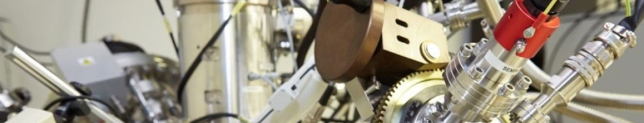
Laser dicer Oxford Lasers A-Series (LASER-DICER)

Guarantor:
Michal Potoček, Ph.D.
Instrument status:
![]() Operational, 9.4.2025 13:34
Operational, 9.4.2025 13:34
Equipment placement:
CEITEC Nano - C1.20
Technologies for ensuring the dies to be properly interconnected and packaged with high precision, accuracy and reliability to eliminate damage of dies and enable easily manipulation. Supporting inspection technologies should provide the possibility of optical surface monitoring and inspection of interconnection and soldering process. Electrical characterization probe station is also planned, as well as temperature dependencies and working stress testing of fabricated dies.
Publications:
-
KOLLER, P.; ASTNER, T.; TISSOT, B.; BURKARD, G.; TRUPKE, M., 2025: Strain-enabled control of the vanadium qudit in silicon carbide. PHYSICAL REVIEW MATERIALS 9(4), p. 46104,772233796 - 46104,772233796, doi: 10.1103/PhysRevMaterials.9.L043201; FULL TEXT
(LASER-DICER) -
Koňařík, L., 2024: Development and fabrication of microelectromechanical systems MEMS. BACHELOR´S THESIS , p. 1 - 46; FULL TEXT
(LASER-DICER, DWL, EVAPORATOR, RIE-FLUORINE, DRIE, NANOCALC, DEKTAK, WIRE-BONDER, LYRA)
Photogallery
Specification
| Laser | Diode-pumped solid state Nd:YAG |
|---|---|
| Wavelength | 532 nm |
| Output | 10W @ 40 kHz |
| Pulse Frequency | 1 – 200 kHz |
Stage
| Lateral range | 200 mm x 200 mm |
|---|---|
| Resolution | 0.5 μm |
| Repeatability | 1 μm |
| Vertical range (maximum sample height) | 56 mm |
Other
This machine is equipped with:
- General purpose clamp jig (incl. wafer up to 4 inches)
- Fume Extractor
- Laser Power meter capable of measuring power up to 20 W
- Machine vision – on-axis alignment camera
- Safety Shutter with interlock circuit
Data for cutting
Your design for cutting should be in DXF format or DWG (saved by AutoCad 2010). We are able to cut through most of solid materials with thickness up to 1 mm.
Silicon wafers can be grooved and then broken manually.
We have hands-on experiences with these materials:
- Silicon wafer – grooving and cutting through (thickness: 525 μm)
- Stainless steel – cutting through (thickness: 600 μm)
- Molybdenum sheet – cutting through (thickness: 1 mm)
Note: Please keep in mind that time of cutting through can be counted in days for thick materials (for example 1 mm molybdenum sheet).
In case you would like to cut any material, please contact guarantor.
Documents
Here is place for your documents.